Double Layer HF PCB - KKPCB
 
HomeTag

Double Layer HF PCB - KKPCB

Double Layer HF PCB – High Frequency Two Layer PCB for RF and Microwave Applications

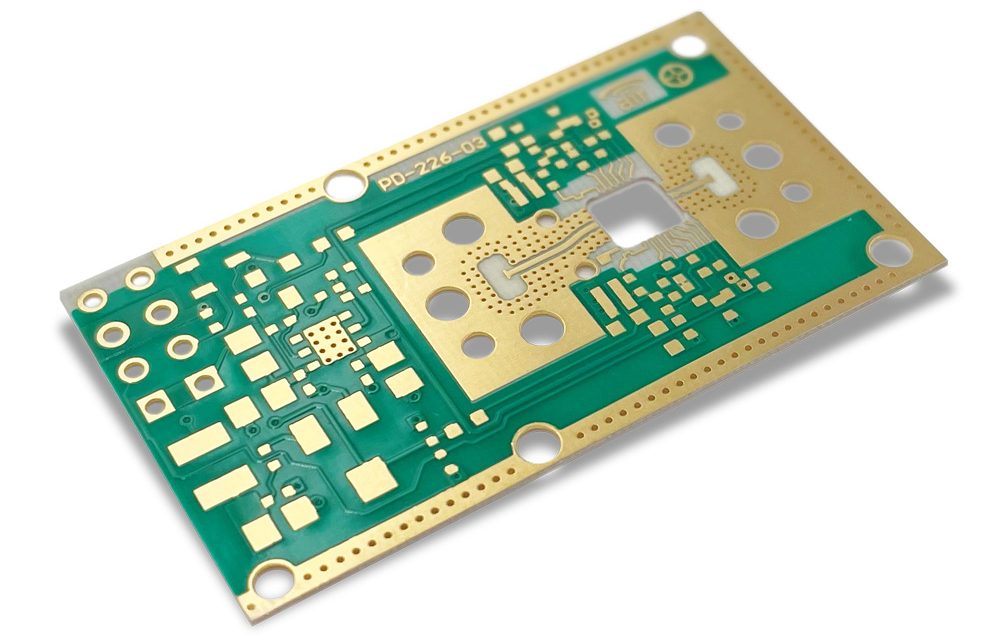
Double Layer HF PCB for RF and Microwave Systems A Double Layer HF PCB (High Frequency PCB) is a two-layer printed circuit board designed specifically for RF and microwave signal transmission. Unlike standard double-sided FR4 boards, HF PCBs use low-loss, stable dielectric materials to ensure reliable signal performance at high frequencies. Double layer high frequency...

Double Layer HF PCB for High Frequency and RF Applications

What Is a Double Layer HF PCB? A Double Layer HF PCB (High Frequency PCB) is a two-layer printed circuit board specifically designed for RF and microwave signal transmission. It uses low dielectric loss materials and optimized trace layouts to maintain signal integrity at high operating frequencies. Compared with multilayer RF boards, double layer HF...

High-Stability Double Layer HF PCB Engineering for Low-Loss RF Routing and Precision High-Frequency Performance

A Double Layer HF PCB is one of the most efficient and cost-optimized architectures for high-frequency designs requiring low-loss transmission, tight impedance control, and stable RF performance up to microwave and lower mmWave ranges. Compared with complex multilayer structures, the Double Layer HF PCB offers a cleaner electromagnetic environment, reduced dielectric loading, and minimized stackup...

Engineering Double Layer HF PCB for Ultra-Stable RF Performance and Low-Loss Microwave Signal Integrity

As RF communication, IoT edge devices, automotive radar, and compact wireless modules continue to evolve, the Double Layer HF PCB has become a preferred architecture for delivering high-frequency stability, low insertion loss, and predictable electromagnetic performance. Although limited to two copper layers, a Double Layer HF PCB—when engineered correctly—can outperform many multilayer structures in signal...

Achieve Low-Loss Transmission and Stable Impedance Performance with Double Layer HF PCB Engineering for High-Frequency Communication Systems

A Double Layer HF PCB may appear structurally simple, yet in high-frequency engineering it provides a remarkably efficient platform for low-loss propagation, stable impedance, and predictable electromagnetic behavior. When RF designers need high-frequency stability without the cost or stackup escalation of multilayer PCBs, a Double Layer HF PCB offers the ideal balance between manufacturability and...