ATE Test PCB - KKPCB
 
HomeTag

ATE Test PCB - KKPCB

Memory Test PCB Manufacturing for DRAM, NAND and High-Speed Memory Testing

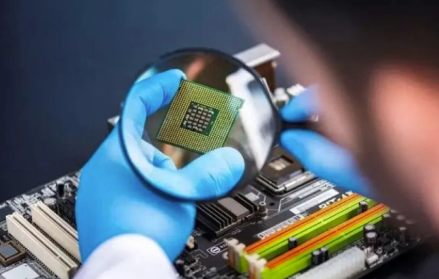
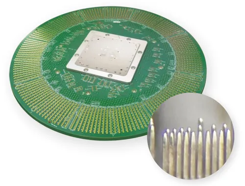
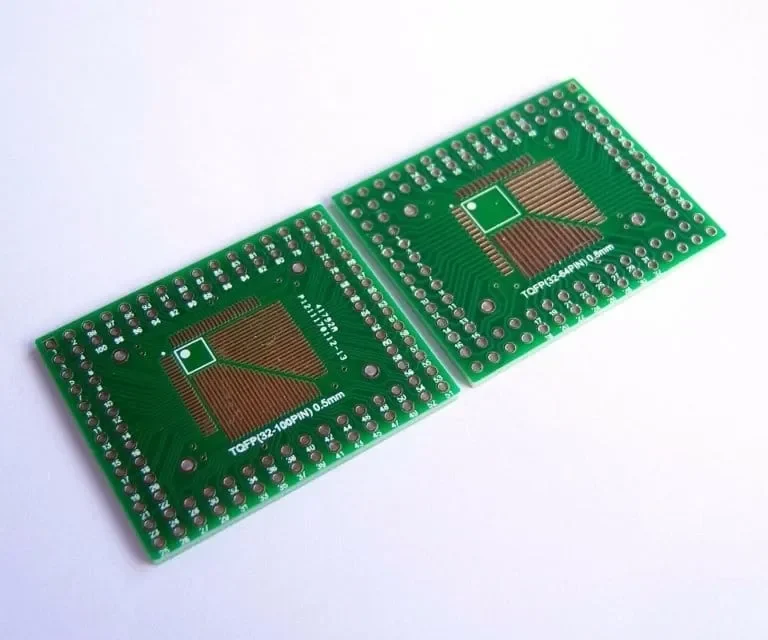
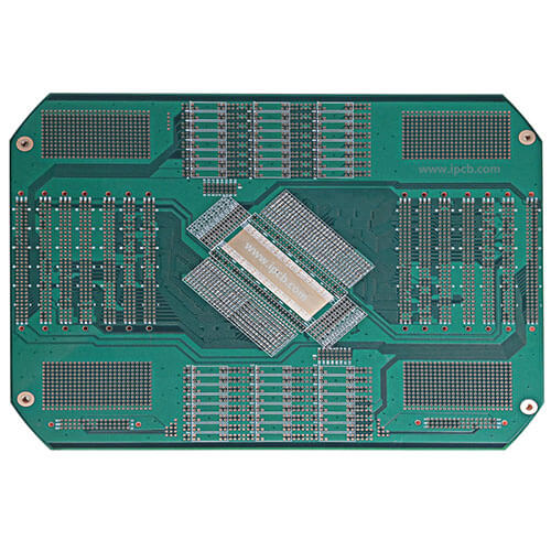
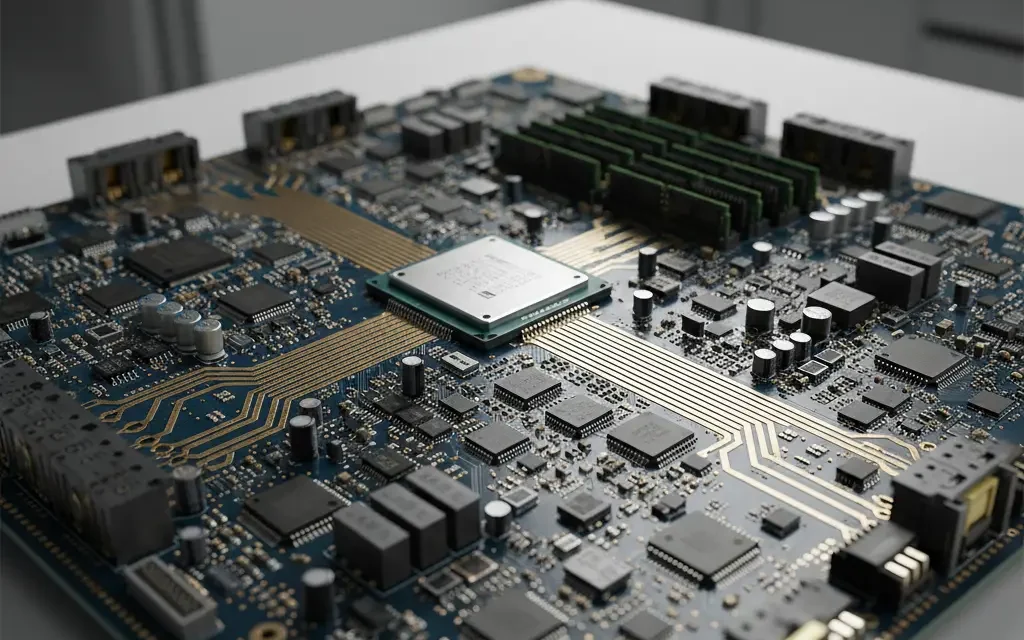
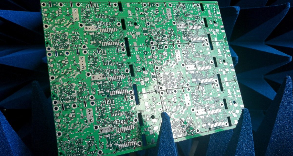
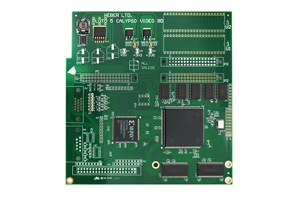
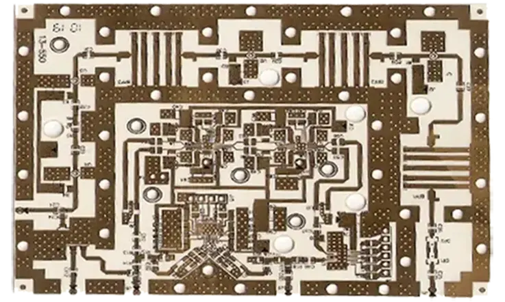
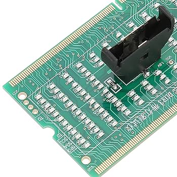
As memory devices continue to evolve toward higher speed, higher density, and lower power consumption, precise testing becomes increasingly critical. A well-designed Memory Test PCB is essential for validating the performance, reliability, and functionality of DRAM, NAND Flash, and other memory ICs throughout development and production stages. Memory test PCBs provide the electrical interface between...

Chip Test PCB Manufacturing for Reliable IC and Semiconductor Testing

As semiconductor devices become faster, smaller, and more complex, accurate testing at the chip level is essential to ensure product performance and yield. A high-quality Chip Test PCB plays a critical role in IC validation by providing a stable and precise electrical interface between the chip under test and automated test equipment (ATE). Chip test...

Wafer Test PCB Manufacturing for Accurate Semiconductor Wafer Testing

In semiconductor manufacturing, wafer testing is a critical step performed before packaging to verify die functionality and performance. A high-quality Wafer Test PCB serves as the electrical interface between the wafer probe card and automated test equipment (ATE), enabling precise signal transmission and accurate measurement results. As IC designs continue to scale in speed, density,...

IC Testing PCB Manufacturing for Reliable Semiconductor Test Applications

As integrated circuits become more complex and performance-driven, IC testing PCB plays a critical role in ensuring functionality, reliability, and yield throughout the semiconductor lifecycle. From early-stage IC validation to high-volume production testing, IC testing PCBs provide the electrical interface between the device under test (DUT) and automated test equipment (ATE). A high-quality IC testing...

Small Batch ATE PCB Manufacturing for Semiconductor and Automated Test Equipment

Small Batch ATE PCB manufacturing is designed to support semiconductor and automated test equipment (ATE) applications that require low-volume production with high performance and reliability. Unlike mass production PCBs, small batch ATE PCBs are typically used for engineering validation, system qualification, pilot runs, and customized test solutions. As test requirements continue to evolve rapidly, small...

ATE PCB Prototype for Semiconductor and Automated Test Equipment

An ATE PCB Prototype is a critical early-stage test board used in automated test equipment (ATE) systems to validate electrical performance, signal integrity, and mechanical compatibility before volume production. In semiconductor testing, a reliable ATE PCB prototype helps reduce development risk, shorten validation cycles, and improve overall test accuracy. As test speeds continue to increase,...

High Speed Test PCB Manufacturer for ATE and Semiconductor Testing

A High Speed Test PCB is a critical interface board used in automated test equipment (ATE) and semiconductor testing systems. As data rates increase and device nodes continue to shrink, high speed test PCBs must support multi-gigabit signal transmission while maintaining excellent signal integrity, impedance accuracy, and electrical stability. Compared with standard test boards, high...

High Pin Count PCB: Advanced PCB Solutions for High-Density and High-Reliability Applications

A High Pin Count PCB is designed to support electronic components with a large number of I/O pins, such as high-density BGAs, processors, FPGAs, and ASICs. As modern electronic systems demand higher performance, faster data transfer, and increased functionality, high pin count devices have become increasingly common. Manufacturing a reliable high pin count PCB requires...

High Frequency Test PCB: Precision PCB Solutions for RF and High-Speed Signal Testing

A High Frequency Test PCB is a critical component in RF, microwave, and high-speed electronic testing environments. As signal frequencies and data rates continue to increase in applications such as 5G communication, mmWave modules, radar systems, and high-speed semiconductor devices, conventional test PCBs can no longer meet accuracy and stability requirements. High frequency test PCBs...

Multilayer Test PCB: High-Reliability PCB Solutions for Advanced Electronic Testing

A Multilayer Test PCB is a critical component used in electronic and semiconductor testing environments, including automated test equipment (ATE), functional testing systems, and reliability validation platforms. As test requirements become more complex and signal speeds increase, multilayer test PCBs are essential for supporting dense routing, stable signal transmission, and long-term mechanical reliability. Professional multilayer...