Advanced PCB Manufacturing - KKPCB
 
HomeTag

Advanced PCB Manufacturing - KKPCB

Buried Via PCB – High Density Multilayer PCB with Internal Via Interconnection

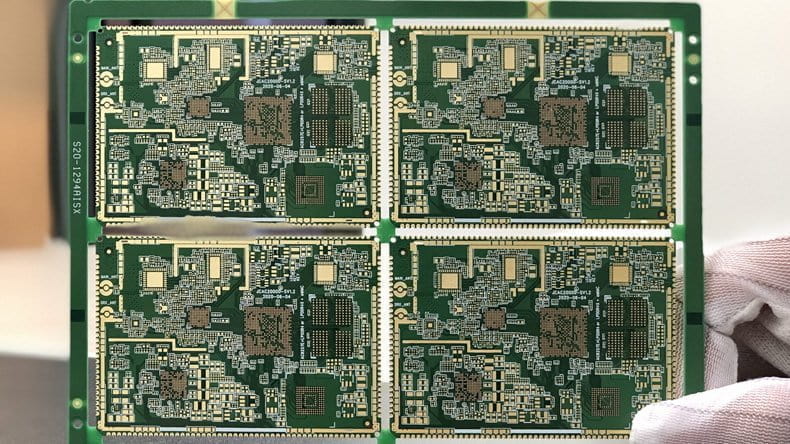
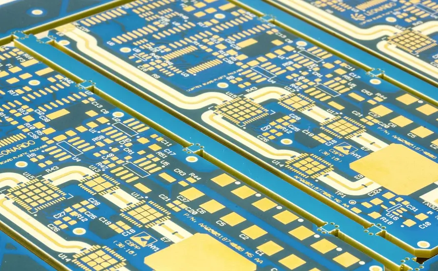
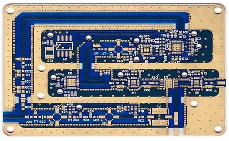
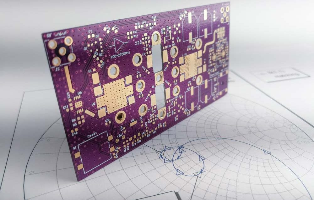
What Is a Buried Via PCB? A Buried Via PCB is a multilayer printed circuit board that uses vias connecting only internal layers, without extending to the outer surface layers. Unlike through-hole vias that pass through the entire board thickness, buried vias are fully embedded within the PCB stack-up. This structure improves routing density, reduces...

Multilayer PCB – High Performance Multi Layer Printed Circuit Board for Advanced Electronics

What Is a Multilayer PCB? A Multilayer PCB is a printed circuit board composed of three or more conductive copper layers laminated together with insulating dielectric materials. Compared to single-sided or double-sided boards, Multilayer PCB technology allows significantly higher circuit density and more complex routing structures. Modern electronic systems increasingly require compact size, high speed...

Fine Pitch PCB – Precision PCB for High Density and Fine Line Applications

What Is Fine Pitch PCB? A Fine Pitch PCB refers to a printed circuit board designed with extremely small trace width and spacing to support high pin count and fine pitch components. It is commonly used in advanced electronic systems where compact design, high integration, and precise routing are essential. Fine pitch designs are typically...

HDI PCB – High Density Interconnect PCB for Advanced Electronics

What Is HDI PCB? HDI PCB (High Density Interconnect PCB) is a printed circuit board designed with higher wiring density per unit area compared to traditional multilayer PCBs. It uses advanced manufacturing technologies such as microvias, blind vias, buried vias, and fine line traces to achieve compact size and improved electrical performance. HDI PCB is...

PTFE PCB Manufacturing for High-Frequency and RF Applications

What Is a PTFE PCB? A PTFE PCB is a printed circuit board made from polytetrafluoroethylene (PTFE) laminates, known for extremely low dielectric loss, stable dielectric constant, and excellent high-frequency performance. PTFE PCBs are widely used in 5G, mmWave modules, RF/microwave systems, aerospace electronics, and high-speed computing, where signal integrity and low insertion loss are...

Rogers PCB Manufacturing for High-Frequency and RF Applications

What Is a Rogers PCB? A Rogers PCB is a printed circuit board that uses Rogers high-frequency laminates, such as RO4003C, RO4350B, and Duroid series, designed for low dielectric loss, precise impedance control, and high-frequency signal transmission. Rogers PCBs are essential in 5G communications, RF/microwave modules, high-speed computing, and aerospace electronics. Why Rogers PCB Technology...

High Frequency Signal PCB Manufacturing for High-Speed and RF Applications

What Is a High Frequency Signal PCB? A High Frequency Signal PCB is a printed circuit board designed to carry high-speed and high-frequency signals with minimal loss, reflection, or distortion. These PCBs are crucial in RF, microwave, 5G, high-speed computing, and semiconductor test applications, where signal integrity and low insertion loss are essential for system...

RF Trace PCB Manufacturing for High-Frequency and Wireless Applications

What Is an RF Trace PCB? An RF Trace PCB is a printed circuit board designed to route high-frequency RF signals with minimal signal loss, reflection, and distortion. These PCBs are optimized for controlled impedance, low insertion loss, and high signal integrity, making them essential for applications such as 5G modules, mmWave systems, wireless communication,...

Differential Pair PCB Design and Manufacturing for High-Speed Data Transmission

What Is a Differential Pair PCB? A Differential Pair PCB is a printed circuit board designed to route differential signal pairs, which are two complementary signals transmitted simultaneously to improve noise immunity, reduce crosstalk, and maintain signal integrity. Differential pair technology is critical in high-speed digital interfaces, such as USB, HDMI, PCIe, Ethernet, DDR memory,...

Fine Line PCB Manufacturing for High-Density and High-Performance Electronics

What Is a Fine Line PCB? A Fine Line PCB is a printed circuit board that uses extremely narrow traces and spaces to support high-density, complex electronic designs. Fine line technology is essential for applications where board real estate is limited but high-speed performance and signal integrity are required, such as smartphones, 5G modules, high-speed...