PCB Materials | FR-4, High-Frequency, Low-Loss & Heavy Copper - KKPCB
 
HomeCategory

PCB Materials | FR-4, High-Frequency, Low-Loss & Heavy Copper - KKPCB

Ceramic PCBs: Optimized for High-Power and High-Frequency Applications

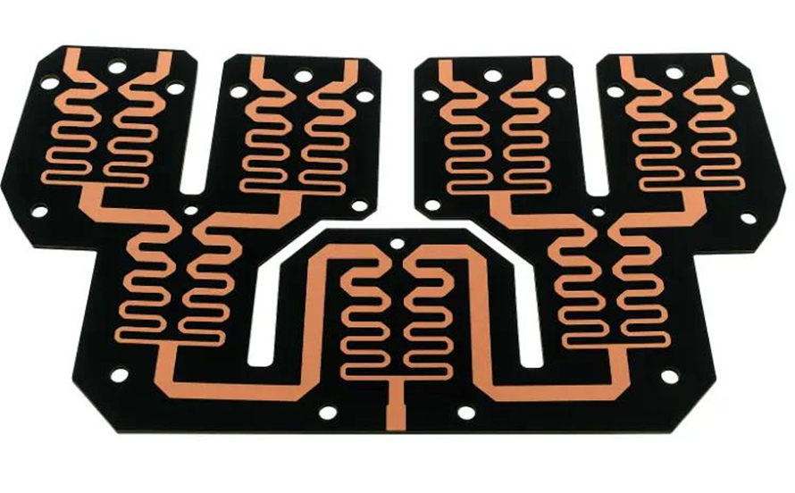
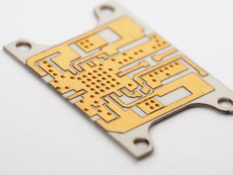
What is a Ceramic PCB? A Ceramic PCB is a printed circuit board built using ceramic substrates like alumina (Al₂O₃), aluminum nitride (AlN), or silicon nitride (Si₃N₄) instead of standard FR-4 or PTFE materials. These substrates are thermally conductive, electrically insulating, and mechanically robust, making them ideal for high-power electronics and RF/microwave applications. Ceramic PCBs...

PTFE PCBs: Ultra-Low Loss Solutions for High-Frequency Electronics

What is a PTFE PCB? A PTFE PCB is a printed circuit board built using polytetrafluoroethylene (PTFE) as the substrate. PTFE is a high-performance polymer renowned for its extremely low dielectric loss (Df), consistent dielectric constant (Dk), and high thermal stability. These characteristics make PTFE PCBs ideal for applications where high-frequency signal integrity and minimal...

Rogers PCBs: High-Frequency Solutions for Advanced Electronic Applications

What is a Rogers PCB? A Rogers PCB is a printed circuit board manufactured using high-performance laminates developed by Rogers Corporation, designed specifically for high-frequency, RF, and microwave applications. Unlike standard FR-4 materials, Rogers substrates offer low dielectric loss (Df), stable dielectric constant (Dk), and superior thermal performance, making them ideal for high-speed and high-frequency...

RF Trace PCBs: Design Principles for High-Frequency Signal Integrity

What is an RF Trace PCB? An RF Trace PCB is a printed circuit board specifically designed to handle high-frequency radio frequency (RF) signals, typically ranging from MHz to GHz and even mmWave frequencies. Unlike standard PCB traces, RF traces must be carefully engineered to behave as controlled transmission lines, ensuring signals propagate with minimal...

Fine Line PCBs: Precision Manufacturing for Ultra-High-Density Electronics

What is a Fine Line PCB? A Fine Line PCB is a printed circuit board designed with extremely narrow trace widths and spacing, typically below 100 microns. These PCBs are essential for high-density electronic designs where space is limited and performance requirements are demanding. Fine line technology is widely used in applications that require compact...

Microvia PCBs: Enabling High-Density and High-Performance Electronics

What is a Microvia PCB? A Microvia PCB is a printed circuit board that uses very small vias—typically less than 150 microns in diameter—to connect adjacent layers. Unlike traditional through-hole or buried vias, microvias enable high-density routing and reduced signal path lengths, making them ideal for high-speed, high-performance, and compact electronic designs. Microvia technology is...

High Reliability PCBs: Design, Manufacturing, and Applications

What is High Reliability PCB? High Reliability PCBs are designed to operate consistently in demanding environments where failure is not an option. These boards are used in aerospace, defense, medical devices, automotive, and industrial systems, where extreme conditions like high temperatures, vibration, humidity, and high-frequency operation can challenge standard PCBs. A High Reliability PCB focuses...

Fine Pitch PCBs: Precision Design for High-Density Components

As electronic devices become smaller and more powerful, the demand for Fine Pitch PCBs—boards designed for components with extremely small pin spacing—has grown significantly. Fine pitch components, such as BGA, QFN, and CSP packages, require precise PCB design and manufacturing to ensure electrical connectivity, signal integrity, and long-term reliability. Design Considerations High-Density Layouts:Fine pitch PCBs...

Low Loss PCBs: Optimizing Signal Integrity for High-Frequency Applications

In modern electronics, especially in RF, 5G, and high-speed communication systems, signal loss can significantly affect device performance. Low loss PCBs are specifically designed to minimize dielectric and conductor losses, ensuring high-frequency signals propagate with minimal attenuation. These PCBs are essential for applications such as mmWave modules, RF transceivers, antennas, and satellite communication systems. Design...

Custom ATE PCBs: Precision Design for Automated Test Equipment

Automated Test Equipment (ATE) plays a vital role in validating electronic components, modules, and systems. At the heart of these test platforms are Custom ATE PCBs, engineered to handle high-speed signals, precise routing, and repeated testing cycles without failure. These PCBs must balance electrical performance, mechanical stability, and long-term reliability to meet stringent testing requirements....