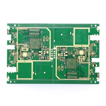
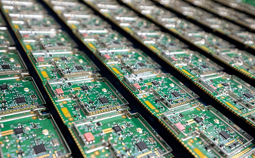
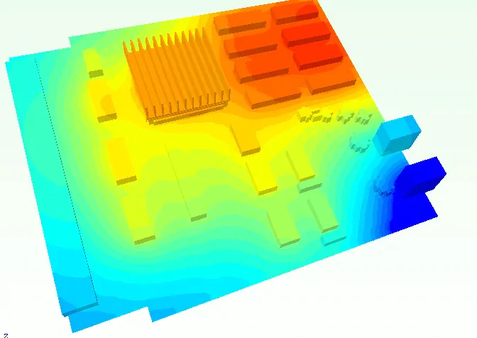
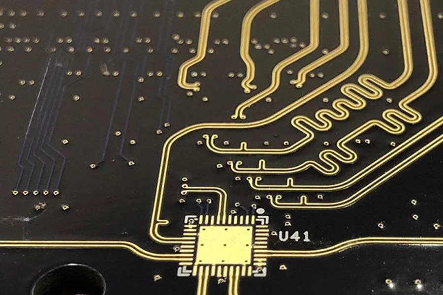
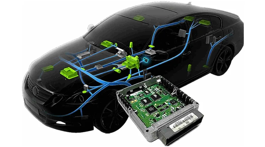
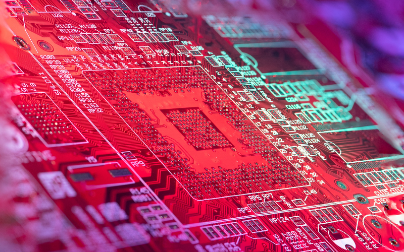
PCB Manufacturing - KKPCB
 
HomeCategory

PCB Manufacturing - KKPCB

The Critical Issue of Near Holes in Multi-Layer PCB Design

In multi-layer PCB design, the primary focus during routing is to ensure efficient and reliable electrical connections between layers using vias. However, as PCB density increases, vias often need to be placed closer together, leading to design and manufacturing challenges. These challenges not only complicate the production process but also impact the long-term reliability of the product....

Experience Sharing in Multi-Layer PCB Impedance Line Routing

With the rapid advancement of modern electronics, devices like smartphones, computers, and high-definition TVs rely heavily on the intricate design of circuit boards to achieve high-speed data transmission. A key component of this functionality is impedance matching, which ensures reliable and stable signal transmission. This article explores practical insights and best practices for impedance-controlled PCB routing,...

High-Speed PCB: Optimal Six-Layer Board Structure

When designing high-speed PCBs, the layer stack-up plays a crucial role in ensuring signal integrity, minimizing crosstalk, and achieving optimal electromagnetic compatibility (EMC). For a standard six-layer board with a thickness of 1.6mm, selecting the right structure can significantly impact performance. Below is an analysis of common six-layer board structures and their suitability for high-speed designs....

Basic Knowledge You Need to Master for PCB Design

PCB design is a critical part of developing electronic systems. It requires knowledge to ensure schematic correctness, signal integrity, minimal interference, and convenient connectivity. Below are key recommendations and optimized methods for PCB design. 1. Working with FPGA If the system involves an FPGA, you must verify the pin assignments using specialized software like Quartus II before creating...

Basic Principles and Operations of PCB Wiring

Wiring Overview and Principles With the rapid development of high-speed circuit design, PCB routing has evolved beyond simple interconnection tasks. Engineers must analyze various distributed parameters using transmission line theory. Distributed parameter circuits account for spatial variations in voltage and current. Modern PCBs, with their complexity and density, include advanced features like microvias, buried/blind vias, and...

Classification and Advantages/Disadvantages of LTCC

LTCC (Low Temperature Co-fired Ceramic) is a special type of ceramic material that integrates multiple ceramic layers together through a co-firing process. With its unique performance advantages, LTCC has found widespread application in circuits and systems operating at microwave, millimeter-wave, and higher frequencies. This article will discuss the classification, advantages, and disadvantages of LTCC in detail....

Features of KLC Series (LTCC Substrate)

Low dielectric loss characteristics (tan δ) and low resistance conductors, low electrical loss, suitable for high-frequency applications Due to our unique manufacturing technology, the size and characteristics of each production batch and within each batch vary little High-density wiring is achieved by improving stacking alignment accuracy Precise control of substrate thickness and cavity shape Resistance,...

Products Wafer-level packaging substrates

The thermal expansion coefficient of these LTCC substrates is adjusted for use as wafer-level packaging substrates. The substrate surface has bumps for electrical connections, and CSP (chip-scale package) can be easily assembled by directly bonding to silicon wafers. Ideal for MEMS and semiconductor ceramic packages with a small number of leads. Features Benefits of using ceramic wafers...

LTCC Multilayer Substrates

KKPCB LTCC substrates with silver conductor material provide multilayer substrates with low dielectric loss. Coils, capacitors and resistors can be embedded in the inner layer. Ideal for high-frequency modules and silicon wafer interposer substrates. Features KKPCB LTCC substrates can embed coils, capacitors and resistors, thereby reducing the substrate size. Excellent dimensional tolerance of ±0.3% improves mounting accuracy. Low conductor...

Ceramic substrates – a complete guide

Shenzhen KKPCB Technology Co., Ltd. is a company that specializes in the design, manufacture, and assembly of various printed circuit boards (PCBs), including ceramic substrates. Below is a comprehensive guide to ceramic substrates as presented by the company: Introduction to Ceramic Substrates Ceramic substrates are advanced materials used in electronic packaging due to their excellent thermal, electrical,...