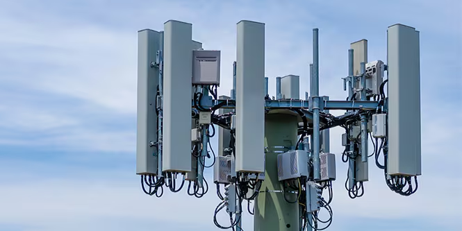
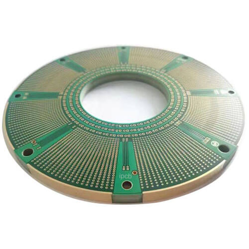
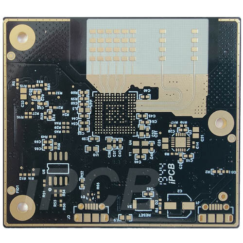
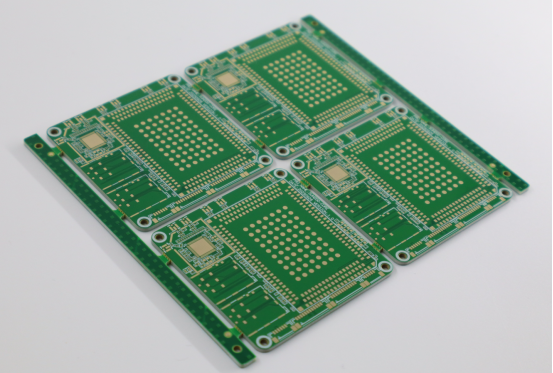
PCB Manufacturing Services | High-Quality PCB & PCBA - KKPCB
 
HomeCategory

PCB Manufacturing Services | High-Quality PCB & PCBA - KKPCB

Enhance Signal Integrity and Thermal Reliability in Multilayer Blind Via PCBs for High-Density RF Modules

High-density RF modules in 5G base stations, satellite payloads, and advanced IoT systems require compact multilayer PCBs with precise signal routing, minimal crosstalk, and high thermal resilience. Blind via technology allows for efficient vertical interconnects while reducing PCB stackup thickness, improving high-frequency performance, and maintaining signal integrity across densely packed layers. KKPCB integrates precision lamination,...

Boost RF Power Handling and Minimize Joule Heating Using Heavy Copper PCB Laminates in High-Power Telecom Amplifiers

High-power telecom amplifiers in 4G/5G base stations, satellite uplinks, and RF power transmitters operate under extreme currents and elevated temperatures. Maintaining low insertion loss, minimized Joule heating, and stable impedance is critical to achieve high RF efficiency, thermal reliability, and signal integrity. Heavy copper PCB laminates (copper thickness 3–6 oz, Dk ~4.0, low Df @10...

Reduce Insertion Loss and Enhance Power Efficiency Using Low Loss PCB Designs for Satellite Communication Payloads

Satellite communication payloads demand high-frequency RF stability, minimal insertion loss, and optimized power efficiency across densely packed multilayer PCBs. Signal integrity degradation, EMI coupling, or thermal hotspots can compromise link margin, telemetry accuracy, and antenna performance. Low loss PCB materials, such as ceramic-reinforced laminates or PTFE-based RF substrates, provide stable dielectric constant (Dk) and low...

Optimize Phase-Stable High-Frequency Routing with Blind Via PCB Architectures in Compact Satellite Communication Payloads

Compact satellite communication payloads require precise, phase-stable RF routing to maintain signal fidelity and low insertion loss across high-frequency channels. The limited space and high-density requirements make blind via architectures essential for multilayer PCBs, enabling signal interconnects without penetrating all layers, reducing parasitic capacitance, and controlling crosstalk. Blind via PCBs allow compact routing of RF...

Accelerate Your PCB Quotation Request for Prototypes and Mass Production with Complete Design Files and Specs

A fast and accurate PCB quotation is critical for electronics designers, hardware engineers, and product managers who are planning prototypes or mass production runs. Providing complete design files and specifications, including Gerber files, Bill of Materials (BOM), PCB layer count, and manufacturing details, allows manufacturers to deliver precise, timely, and optimized PCB pricing. Without complete...

Improve Multi-Gigabit Transmission and Low-Loss Routing Through Impedance Controlled PCB Engineering for Data Center Switches

Modern data center switches demand high-speed, multi-gigabit transmission across densely packed PCB layers. Maintaining low insertion loss, tight impedance control, and minimal crosstalk is critical to guarantee reliable signal integrity, reduce latency, and preserve network throughput. Impedance-controlled PCB architectures provide predictable high-frequency performance for differential pair routing and dense multilayer stackups. KKPCB leverages precision lamination,...

Optimize RF Signal Integrity and Lightweight HDI UAV PCB Architectures for Next-Gen Drone Navigation Modules

Next-generation UAV systems—whether used for industrial IoT sensing, long-range inspection, autonomous mapping, or precision agriculture—depend on PCB platforms capable of delivering high-frequency RF accuracy, ultra-stable GNSS/GPS reception, multi-band communication reliability, and lightweight HDI construction. As flight durations extend and sensor payloads grow more complex, the PCB becomes the backbone that determines navigation precision, RF sensitivity,...

Unlock Ultra-Stable RF Propagation and Low-Loss Routing with Next-Gen Multilayer HF PCB Platforms for Dense mmWave Arrays

Dense mmWave arrays, commonly used in 5G massive MIMO, radar, and satellite phased arrays, require ultra-stable RF propagation, minimal insertion loss, and precise impedance control across multilayer interconnects. Thermal stress, mechanical vibration, and high-frequency crosstalk can severely degrade signal fidelity, phase alignment, and overall array performance. Next-generation multilayer HF PCB platforms leverage advanced dielectric laminates...

Boost High-Q Resonance and Ultra-Stable Impedance Control with High-Frequency Sensor PCB Structures for Aerospace Navigation Sensors

Aerospace navigation sensors operate in a realm where the margin for error is essentially zero. Whether guiding autonomous aircraft, stabilizing flight control modules, or supporting satellite-assisted positioning, these sensors rely on high-frequency PCB platforms engineered for absolute electrical stability. Achieving high-Q resonance and ultra-consistent impedance is not just a design preference—it is the foundation of...

Reinforce Shock Reliability and High-Frequency Integrity Through Ruggedized mmWave Module PCB Designs for Harsh-Environment Communication Terminals

Harsh-environment communication terminals—used in battlefield radios, mining telemetry units, emergency response networks, and remote industrial gateways—depend on mmWave Module PCB architectures that can preserve signal integrity, impedance accuracy, and structural reliability under extreme stress. High-frequency circuits operating from 24 GHz to 71 GHz experience sensitivity far greater than conventional RF PCB designs, making material stability,...