PCB Assembly (PCBA) Services | Turnkey Solutions - KKPCB
 
HomeCategory

PCB Assembly (PCBA) Services | Turnkey Solutions - KKPCB

RF-35 PCB: A Reliable Low-Loss Material for High-Frequency RF Applications

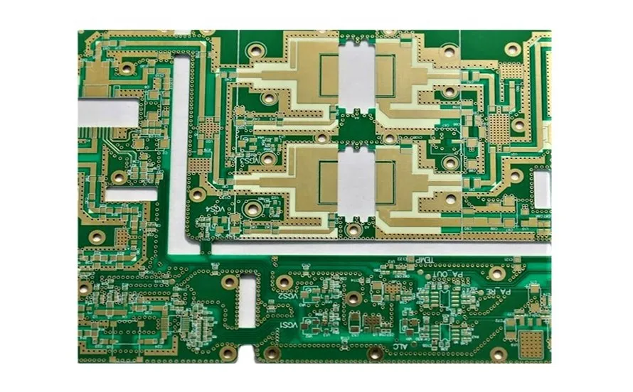
As wireless communication technologies continue to evolve, the demand for reliable high-frequency PCB materials has increased significantly. Applications such as RF communication systems, antennas, radar modules, and microwave devices require PCB substrates that provide stable electrical performance and low signal loss. One widely used solution in RF circuit design is the RF-35 PCB, a high-frequency...

Low Loss PCB for High-Frequency and High-Speed Signal Applications

As modern electronic systems operate at increasingly higher frequencies and faster data rates, signal loss has become a major challenge in PCB design. Low Loss PCBs are specifically engineered to minimize signal attenuation and maintain signal integrity in high-speed and high-frequency circuits. Unlike conventional FR-4 boards, low loss PCBs use advanced dielectric materials with lower...

Small Batch ATE PCB Manufacturing for Semiconductor and Automated Test Equipment

Small Batch ATE PCB manufacturing is designed to support semiconductor and automated test equipment (ATE) applications that require low-volume production with high performance and reliability. Unlike mass production PCBs, small batch ATE PCBs are typically used for engineering validation, system qualification, pilot runs, and customized test solutions. As test requirements continue to evolve rapidly, small...

Burn-in PCB Design and Manufacturing for High-Temperature Semiconductor Reliability Testing

A Burn-in PCB is a specialized test interface designed for accelerated semiconductor reliability screening under sustained electrical and thermal stress. In burn-in systems, the PCB is exposed to continuous high temperature, elevated voltage, and long operating cycles, making it one of the most mechanically and electrically stressed PCB types in semiconductor test environments. Unlike functional...

Selecting an ATE PCB Supplier for High-Performance Automated Test Equipment Applications

An ATE PCB (Automated Test Equipment PCB) is a specialized circuit board designed to interface with test instrumentation for semiconductor devices, modules, and high-speed systems. A reliable ATE PCB supplier plays a critical role in ensuring signal integrity, mechanical precision, and long-term reliability in high-volume testing environments. Importance of High-Quality ATE PCBs ATE PCBs must...

Probe Card Assembly PCB: Precision PCBs for Wafer-Level Semiconductor Testing

A Probe Card Assembly PCB is a critical semiconductor test PCB used in wafer-level testing to provide the electrical and mechanical interface between Automated Test Equipment (ATE) and semiconductor wafers. It supports probe needles or MEMS probes, routing test signals with extreme precision to ensure accurate electrical characterization before wafer dicing and packaging. As semiconductor...

Test Socket PCB for IC: High-Precision PCBs for Reliable IC Socket Testing

A Test Socket PCB for IC is a specialized semiconductor test PCB used to mount and interface IC test sockets within Automated Test Equipment (ATE) systems. Acting as the electrical bridge between the tester and the device under test (DUT), the test socket PCB ensures reliable signal transmission, stable power delivery, and consistent mechanical alignment...

Semiconductor Load Board: High-Performance PCBs for Accurate ATE IC Testing

A Semiconductor Load Board is a specialized ATE test PCB that serves as the electrical interface between Automated Test Equipment (ATE) and the device under test (DUT). Load boards route signals, power, and control lines from the tester to the IC through test sockets, enabling precise functional and parametric testing during semiconductor validation and mass...

Probe Card Assembly PCB: Precision PCB Solutions for Wafer-Level Semiconductor Testing

A Probe Card Assembly PCB is a highly specialized semiconductor test PCB used in wafer-level testing to electrically interface between Automated Test Equipment (ATE) and semiconductor wafers. As the core structure of a probe card, this PCB supports probe needles, MEMS probes, or vertical probe arrays, ensuring precise signal transmission and reliable mechanical alignment during...

Automated Test Equipment PCB: High-Reliability PCBs for Precision Semiconductor Testing

An Automated Test Equipment PCB is a critical component used in ATE systems to perform functional, parametric, and reliability testing of semiconductor devices. These PCBs serve as the electrical interface between the test system and the device under test (DUT), ensuring accurate signal transmission, stable power delivery, and reliable measurement during high-volume semiconductor testing. As...