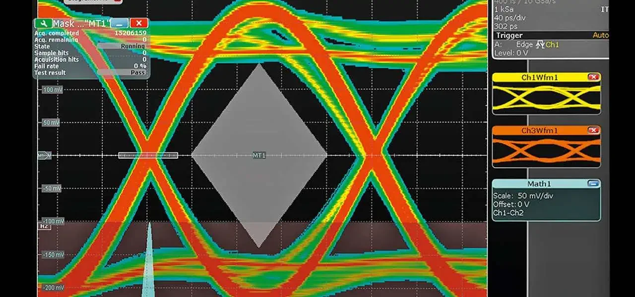
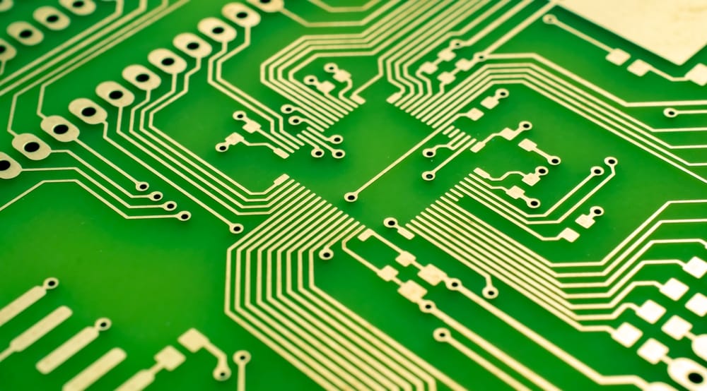
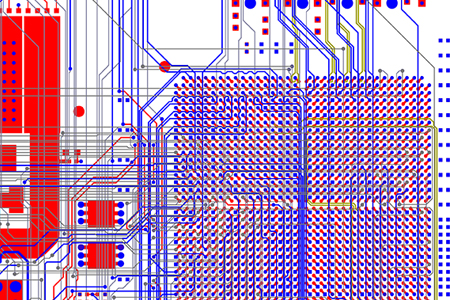
Advanced Engineering Technologies for PCB & PCBA Solutions - KKPCB
 
HomeCategory

Advanced Engineering Technologies for PCB & PCBA Solutions - KKPCB

Rogers high frequency circuit board uses 24GHz radar and 77GHz radar detection observation

24GHz radar detection system mainly supports short-range detection (SRR), high frequency circuit board and high wavelength. Applicable boards: RO4835, RO4350B, RO4003C . Among them, RO4350B nitride ceramic laminate and RO4835 nitride ceramic laminate are highly recommended. These two series belong to the cost-effective series for people’s daily use. Its PCB production cost is low, and it has...

How to distinguish whether a PCB is single-layer or double-layer?

PCB physical object: A double-layer board has copper foil conductors on both sides. Electronic version PCB: There are two colors of conductors (different colors of conductors represent different layers) 3 Double-layer PCB board design and wiring principles The ground wire of the double-layer board is designed to be formed as a grid-shaped frame, that is, more parallel ground wires are laid...

Comprehensive Electronic Components Sourcing Service at KKPCB

At KKPCB, we offer reliable electronic components sourcing, streamlining the process for you. Send us your BOM, and we’ll handle everything, eliminating the need for you to compare prices and sources. Why Choose KKPCB? Beyond PCB manufacturing, we specialize in component sourcing. Unlike many providers, our internal purchasing department ensures a seamless process, working with trusted distributors like...

PCB design technologySetting Up the PCB Design Software Environment: A Comprehensive GuidePCB design technology

Software Rule Settings To begin with, enter Design > Rules and adjust the options based on design requirements: Safety Spacing Settings: In PROTEL99SE, the Clearance Constraint under Routing defines the necessary spacing between traces, pads, and vias of different networks. Single/Double-sided boards: Set spacing to 10-12mil. Multi-layer boards (four layers or more): Set spacing to 6-8mil. Routing Layer and Direction: Go to Routing Layers under Routing and set...

4 Special Electroplating Methods in Circuit Board Welding

In circuit board manufacturing, various electroplating methods are employed to enhance performance, durability, and contact quality. This article focuses on four specialized electroplating methods commonly used in PCB (printed circuit board) welding processes. 1. Finger-Ring Electroplating Finger-ring electroplating involves plating rare metals, such as gold, on the edge connectors or gold fingers of circuit boards to provide low...

Eight Common Circuit Design Misunderstandings You Must Know

In circuit design, there are often principles that engineers assume to be correct, but in reality, they may lead to issues in performance or efficiency. Here are eight common circuit design misunderstandings every electronics engineer should be aware of: Misunderstanding 1: Thin Wires and Automatic Routing Are Good Enough for Low-Requirement PCB Design Comment: While automatic routing might...

Understanding and Improving PCB Open Circuits: Causes and Solutions

Open circuits and short circuits are common issues that PCB manufacturers encounter, often leading to shipment delays, customer complaints, and costly production interruptions. With over 20 years of experience in the PCB manufacturing industry—covering production, quality management, process optimization, and cost control—I have gathered valuable insights into addressing these challenges. Below is a summary of the main causes of PCB...

PCB Drawing: A Summary of Key Practices from Years of Experience

After years of experience in PCB design, certain best practices have emerged. Here, we outline essential aspects of PCB layout, wiring, copper plating, and more, with a focus on optimizing performance and manufacturability. 1. Layout and Wiring Impact on Electrical Performance Separate Digital and Analog Ground: Although challenging, separating these can reduce noise. Understanding IC electrical...

Key Grounding Techniques in Electronic Design

Grounding is fundamental in electronic PCB circuit design, influencing stability, noise immunity, and overall performance. Grounding techniques range from basic single-loop analog grounding to advanced grounding methods for complex mixed-signal designs. These techniques become increasingly critical in high-frequency or high-EMC (Electromagnetic Compatibility) environments. Here’s a comprehensive overview of grounding techniques and methods for reducing ground loops to enhance...

Detailed explanation of three special PCB wiring methods

Before explaining the inspection work after PCB wiring is completed, we will first introduce three special PCB routing techniques. The routing of PCB LAYOUT will be explained from three aspects: right-angle routing, differential routing, and serpentine routing: Right-angle routing (three aspects) The impact of right-angle routing on signals is mainly reflected in three aspects: first, the corner...