Advanced Engineering Technologies for PCB & PCBA Solutions - KKPCB
 
HomeCategory

Advanced Engineering Technologies for PCB & PCBA Solutions - KKPCB

Heavy Copper PCB – High Current and High Reliability PCB for Power Applications

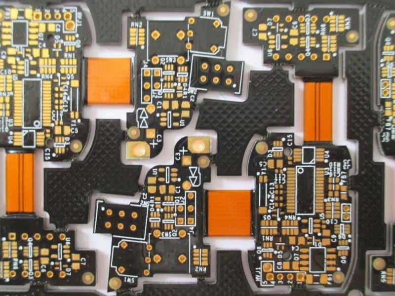
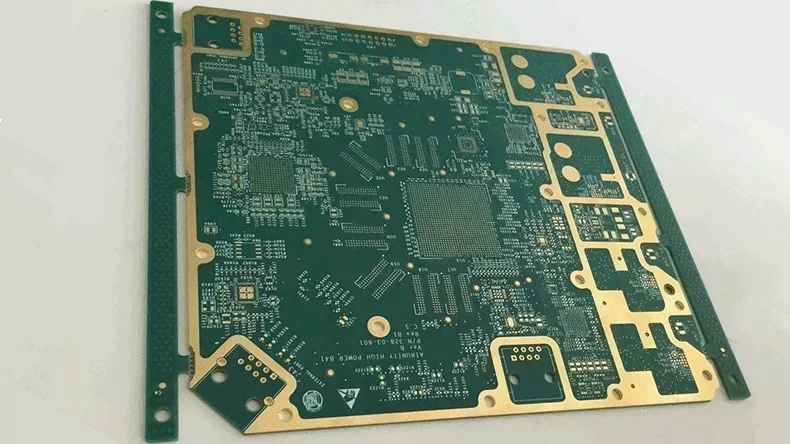
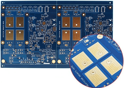
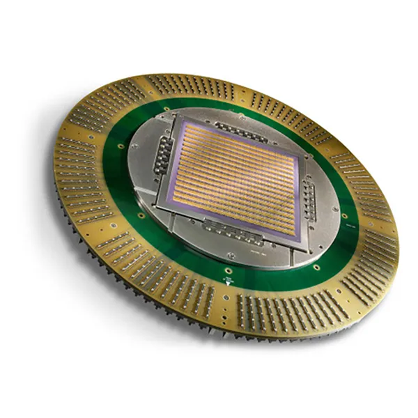
What Is a Heavy Copper PCB? A Heavy Copper PCB is a printed circuit board manufactured with thick copper layers, typically 3 oz/ft² and above. In some high-power applications, copper thickness can reach 10 oz, 20 oz, or even more depending on current requirements. Unlike standard 1 oz copper PCBs, heavy copper boards are designed...

Robotics PCB – High Reliability Control and Power PCB Solutions for Intelligent Robotic Systems

What Is a Robotics PCB? A Robotics PCB is a printed circuit board designed to support the control, sensing, communication, and power management functions of robotic systems. Unlike standard control boards, robotics PCBs must integrate multiple subsystems within limited space while maintaining electrical stability and mechanical durability. They serve as the electronic backbone of modern...

SiC PCB – High Temperature and High Power PCB Solutions for Silicon Carbide Applications

What Is a SiC PCB? A SiC PCB is a printed circuit board specifically designed to support Silicon Carbide (SiC) power devices. SiC semiconductors operate at higher voltages, higher temperatures, and higher switching frequencies compared to traditional silicon devices. Because of these characteristics, the PCB supporting SiC components must provide superior thermal management, electrical insulation,...

High Speed PCB – Optimized Signal Integrity Design for High Data Rate Systems

What Is a High Speed PCB? A High Speed PCB is a printed circuit board specifically designed to support high data rate digital signals. As signal edge rates become faster and transmission speeds reach multi-gigabit levels, PCB layout and stack-up design directly affect signal integrity. High-speed PCB design focuses on maintaining clean signal transmission while...

High TG PCB for Multilayer and High Thermal Stress Applications

A High TG PCB refers to a printed circuit board manufactured with laminate materials that feature a high glass transition temperature, typically 170°C or above. However, in advanced electronics, High TG material selection is not only about temperature tolerance — it is fundamentally about mechanical stability under thermal stress. In multilayer, thick copper, and high-power...

Probe Card PCB – High Precision Interface Board for Wafer-Level Semiconductor Testing

What Is a Probe Card PCB? A Probe Card PCB is a high-precision printed circuit board used in semiconductor wafer-level testing. It serves as the electrical interface between Automated Test Equipment (ATE) systems and the wafer under test. Unlike load boards used for packaged ICs, probe card PCBs are specifically designed to connect to microscopic...

ATE Test PCB – High Reliability Test Board for Automated Test Equipment Systems

What Is an ATE Test PCB? An ATE Test PCB is a specialized printed circuit board used in Automated Test Equipment (ATE) systems to perform functional, parametric, and reliability testing of semiconductor devices. ATE test boards act as the electrical interface between the testing machine and the device under test (DUT). They ensure accurate signal...

5G IC Test PCB – High Frequency Test Board for 5G RF and High-Speed Chip Validation

What Is a 5G IC Test PCB? A 5G IC Test PCB is a specialized printed circuit board designed for functional testing, RF validation, and high-speed performance verification of 5G integrated circuits. Unlike standard application PCBs, test PCBs are engineered to provide stable signal paths, accurate impedance control, and minimal insertion loss during chip evaluation...

Multilayer PCB – Advanced Layered Circuit Board for High-Performance Electronic Systems

What Is a Multilayer PCB? A Multilayer PCB is a printed circuit board consisting of three or more conductive copper layers laminated together with insulating dielectric materials. These layers are electrically interconnected through plated vias to create complex routing structures within a compact footprint. Compared to single-layer or double-layer boards, multilayer PCBs enable higher circuit...

Microvia PCB – Laser-Drilled HDI Technology for High-Density Interconnection

What Is a Microvia PCB A Microvia PCB is a high-density interconnect (HDI) printed circuit board that uses laser-drilled microvias to connect adjacent copper layers. Unlike traditional mechanical through-holes, microvias are extremely small and typically connect only one or two layers. Microvia technology enables higher routing density, improved electrical performance, and more compact electronic designs....