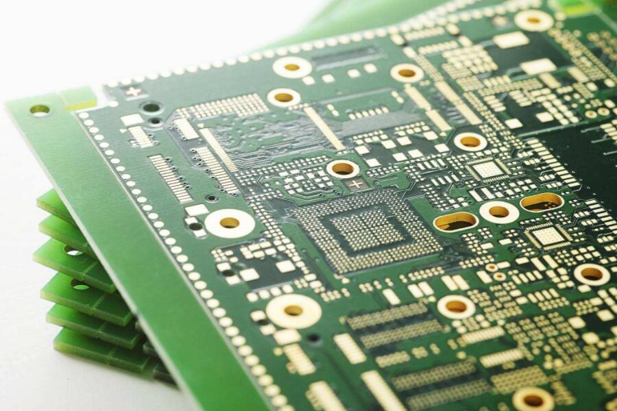
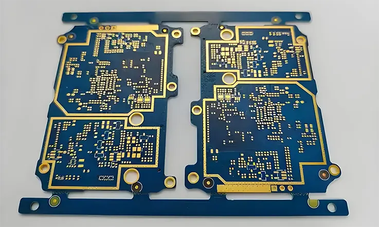
Advanced Engineering Technologies for PCB & PCBA Solutions - KKPCB
 
HomeCategory

Advanced Engineering Technologies for PCB & PCBA Solutions - KKPCB

Standard PCB Thickness and Optimization

When designing a printed circuit board (PCB), engineers often focus on ensuring the correct impedance structures and electrical performance of the board. However, the physical characteristics, such as PCB thickness, are equally important and can significantly impact the cost, manufacturability, and performance of the final product. While standard PCB thicknesses are widely used, they are more of a...

PCB Design For Military & Aerospace Applications

Military and aerospace PCBs must adhere to intensely high standards to ensure their safety and functionality in the extreme conditions they’re used in. For this reason, PCB design for military and aerospace applications requires incredibly stringent guidelines with built in redundancy, extra safety, and stringent tolerances, minimizing risk of failure. General PCB Design Tips for Military and Aerospace Applications...

Low Power Circuit Design Strategies for PCBs

Low power circuit design includes strategies focused on minimizing both dynamic and static power usage in your printed circuit boards. While selecting components with low power requirements is a crucial element, low power PCB design involves more comprehensive considerations to effectively manage power consumption. Lower Power Circuit Designs Tips Aspect Description Identify Major Power Consumers Start by...

RF Via Transitions in High-Speed Designs: Best Practices and Considerations

In high-speed and RF PCB designs, controlling trace impedance is critical, but the role of RF via transitions is often underestimated. Vias, which connect signals between layers, can introduce impedance mismatches, signal reflections, and losses, especially at high frequencies. Proper design and optimization of via transitions are essential to maintain signal integrity and ensure reliable performance in RF and...

How to Check for PCB Warpage: Techniques and Methods

PCB warpage is a common issue caused by stress during the PCB construction process, where the board undergoes expansion and contraction, leading to internal stress and deformation. Detecting PCB warpage early in the assembly stage is crucial, as it can negatively impact printing, mounting, and soldering processes. Warpage can lead to problems such as component misalignment, poor solder...

How to Find Faulty Components on PCBs: A Comprehensive Guide

Troubleshooting printed circuit boards (PCBs) can be a daunting task, but with a systematic approach, it becomes manageable and efficient. This guide provides a step-by-step process to identify faulty components on PCBs, along with methods tailored to specific component types and advanced techniques for batch inspection. Step-by-Step Guide to Finding Faulty Components on PCBs Step 1: Power...

Exploring the Current Carrying Capacity of Flexible PCBs

Flexible PCBs, commonly made from polyimide materials, are known for their amber color and ability to withstand high temperatures, often comparable to or exceeding those of FR4 boards. The current carrying capacity of flexible PCBs is primarily determined by factors such as copper thickness, trace width, and material properties. With a relative tracking index (CTI) typically above 600 volts, these PCBs are suitable for...

Optimizing PCB Trace Thickness vs. Current Capacity

The relationship between PCB trace thickness and current capacity is a critical aspect of PCB design. Properly sizing traces ensures that they can handle the required current without overheating, which is essential for the reliability and functionality of the circuit. This article explores the key considerations for selecting trace thickness, the impact of copper weight, and...

PCB Routing: Best Practices for Ensuring Signal Integrity and Performance

Printed Circuit Board (PCB) routing is a critical aspect of electronic design, ensuring that electrical signals are transmitted efficiently and reliably between components. Proper routing minimizes interference, maintains signal integrity, and meets design requirements such as impedance control and thermal management. This article outlines the best practices for PCB routing, focusing on optimizing performance and ensuring signal integrity....