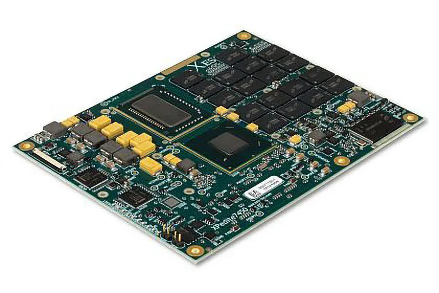
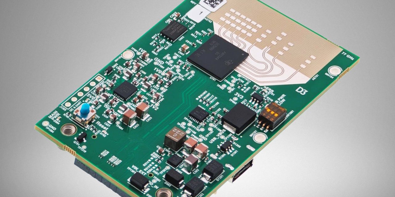
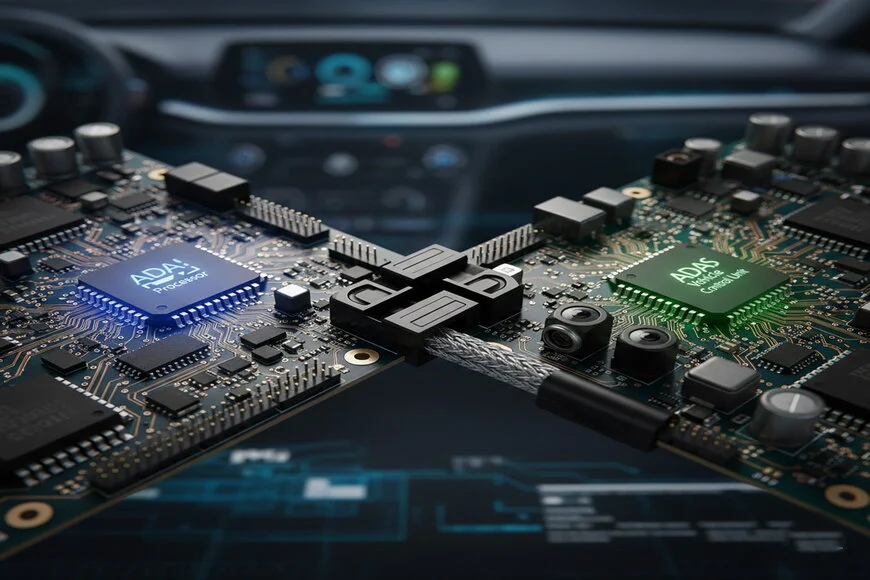
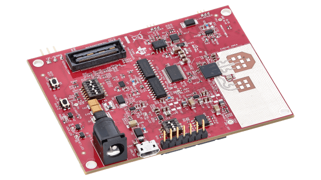
Advanced Engineering Technologies for PCB & PCBA Solutions - KKPCB
 
HomeCategory

Advanced Engineering Technologies for PCB & PCBA Solutions - KKPCB

Common Problems and Solutions for Substrates in PCB Design

The following outlines major issues encountered with substrates in PCB design, including their symptoms, possible causes, inspection methods, and solutions. 1. Soldering Problems Phenomenon: Cold solder joints or solder joints with blowout holes. Inspection Method: Analyze holes before and after dip soldering to identify copper stress points. Perform rigorous incoming material inspections on raw substrates. Possible Causes:...

PCB Interconnection Methods

The interconnection of electrical contacts between components and electromechanical parts in a PCB ensures the system functions as per the circuit schematic. Selecting an appropriate interconnection method depends on the specific application, balancing reliability, processability, and cost. Below are commonly used PCB interconnection methods, along with their advantages, considerations, and application scenarios. 1. Soldering Method This...

PCB Manufacturing Packaging Process

Proper packaging plays a crucial role in ensuring the safe delivery of PCBs, particularly in competitive markets where quality and presentation are key factors. Though packaging may not generate direct added value, it impacts customer satisfaction and reflects professionalism, particularly for high-precision products like PCBs. This article discusses the importance of packaging, the evolution of...

5 Key Points in PCB Design for Power Supply Applications

In power supply design, PCB layout plays a critical role in ensuring the circuit’s efficiency, stability, and reliability. Below are five essential considerations for effective PCB design in power supply applications: 1. Establish a Logical and Linear Signal Flow Directionality is crucial in PCB design to minimize interference and ensure smooth operation. Segregation of Signals: Separate input/output, AC/DC, strong/weak signals,...

Essentials of PCB Design: Grounding Considerations

Grounding is a critical aspect of PCB design, particularly in mixed-signal environments where digital and analog circuits coexist. Proper grounding ensures stable performance, minimizes noise, and improves the reliability of the overall circuit. Below are key insights and guidelines to address grounding challenges effectively. Key Grounding Concepts Analog Ground (AGND) vs. Digital Ground (DGND): Purpose: Separate analog...

Factors Affecting the Quality of PCB SMT Laser Steel Mesh

1. Manufacturing Process The best manufacturing process includes electropolishing after laser cutting. Processes like chemical etching and electroforming are prone to errors, such as issues in film making, exposure, or substrate unevenness. 2. Materials Used Steel Mesh Frame: Must withstand a degree of pressure and maintain levelness. Screen: Polyester mesh is ideal for long-term stable tension. Steel Sheet: Type 304 matte finish is preferred...

Classification and Parameters of PCB Board Materials: Comprehensive Guide

Overview of PCB Materials Printed Circuit Boards (PCBs) are fabricated using various materials to meet specific performance and application requirements. In China, PCB copper-clad laminates (CCLs) are extensively used, and they can be categorized by base materials, resin adhesives, flame retardancy, and performance levels. Types of Copper-Clad Laminates (CCLs) 1. Classification by Reinforcement Material Paper-based materials: Typically used for low-cost...

High-Speed PCB Design Guide XI: How to Improve Testability

As electronic devices become increasingly miniaturized, advancements in component and wiring technologies have created new challenges for production testing. Highly integrated ICs, smaller insulation spacings, and limited access to circuit nodes have made traditional testing methods insufficient. To address these challenges, a design-for-testability (DFT) approach is essential to reduce testing costs and enhance production efficiency. This...

High-Speed PCB Design Guide 9: Mastering IC Packaging Characteristics

Electromagnetic interference (EMI) control is critical in high-speed PCB design, and one often-overlooked aspect is the influence of integrated circuit (IC) packaging. Incorporating decoupling capacitors within the IC package can effectively reduce EMI and enhance signal integrity. This guide delves into the role of IC packaging in EMI suppression, exploring the root causes of EMI, key IC package design...

High-Speed PCB Design Guide 8: PCB Reliability Design

Printed circuit boards (PCBs) remain the backbone of electronic assembly across various systems. Even with perfectly designed schematics, poor PCB design can significantly compromise reliability. For instance, closely spaced thin parallel lines on a PCB can cause signal waveform delays and reflected noise at transmission line terminals. This guide outlines essential considerations for designing reliable PCBs. 1. Ground Wire...