KKPCB Blog – PCB & PCBA Insights, News, and Tips - KKPCB
 

Blog

Explore the KKPCB Blog for the latest PCB manufacturing and assembly news, industry insights, expert tips, and technology trends, helping you stay informed and optimize your electronics projects.
RF Test PCB: Engineering Precision for High-Frequency Testing Systems

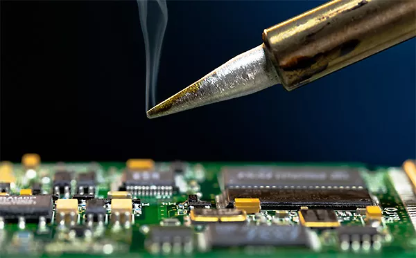
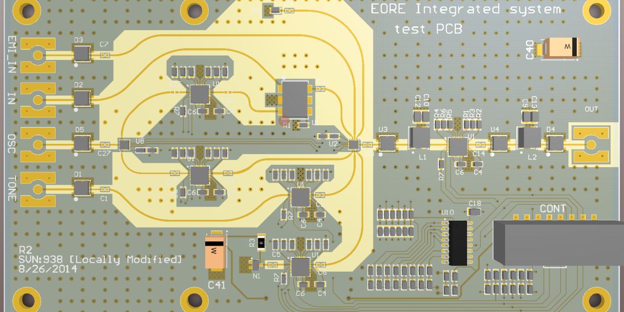
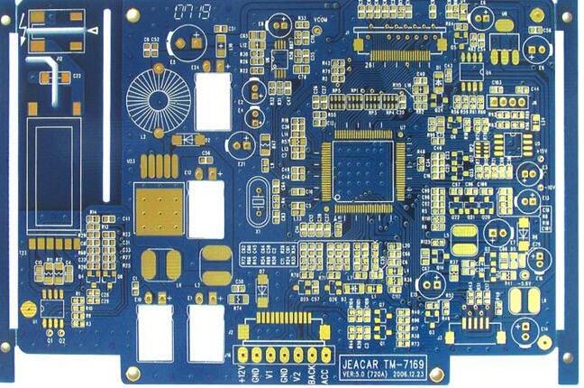
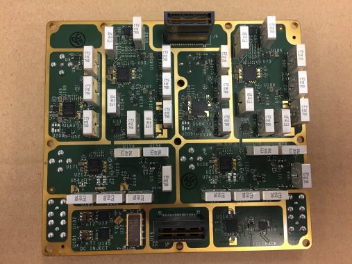
RF Test PCB: Engineering Precision for High-Frequency Testing Applications Introduction As wireless communication, semiconductor devices, and high-frequency electronics continue to advance, the demand for precise and reliable test platforms has increased dramatically. Among these platforms, the RF Test PCB plays a central role. It enables engineers to validate RF performance, measure high-frequency characteristics, and ensure...

Aluminum Oxide (Al₂O₃) Ceramic PCB: Properties, Types, Manufacturing Process, and Industry Applications

Introduction to Aluminum Oxide (Al₂O₃) Ceramic PCBs In the field of printed circuit board (PCB) manufacturing, the choice of substrate material plays an essential role in determining the product’s performance, reliability, and heat dissipation capability. Ceramic PCBs—particularly those using Aluminum Oxide (Al₂O₃)—have become increasingly popular due to their outstanding thermal and electrical properties. This article...

Probe Card PCB: Engineering Precision for High-Accuracy Wafer-Level Semiconductor Testing

Probe Card PCB: Engineering Precision for Wafer-Level Testing Introduction At the wafer-level test stage, the probe card PCB serves as the indispensable interface between automated test equipment (ATE) and the semiconductor wafer. As device geometries continue shrinking and electrical performance requirements become more demanding, precision test interfaces have become essential. The probe card PCB establishes...

ADAS PCB Layout Guidelines for Automotive Radar Systems: Best Practices for High-Frequency Design

ADAS PCB Layout Guidelines for Automotive Radar Systems In the rapidly advancing world of automotive technology, Advanced Driver Assistance Systems (ADAS) are revolutionizing how we drive, enhancing safety and intelligence in vehicles. At the heart of many ADAS features lies the automotive radar system, which relies on precise and effective printed circuit board (PCB) design...

Signal Integrity Optimization and Phase Stability of RF-35 PCB Boards in Precision RF Test & Measurement Equipment

1. Introduction   In advanced RF and microwave test systems, where signal accuracy defines measurement integrity, the substrate material directly determines consistency.  The RF-35 PCB—a low-loss laminate with optimized dielectric uniformity—has become a preferred platform for network analyzers, calibration modules, and power sensors operating between 20 GHz to 50 GHz.  KKPCB’s engineering framework addresses key...

Comprehensive Guide to Flux Application in PCBA: Coating Methods, Process Characteristics, and Key Usage Points

Flux is the “unsung hero” in the PCBA (Printed Circuit Board Assembly) process, directly affecting solder joint quality, production efficiency, and product reliability. Understanding flux application methods, process characteristics, and key precautions is essential for any electronics manufacturer. This guide explores these aspects to help engineers optimize flux application in PCBA. I. Four Mainstream Flux...

Rigid-Flex PCB Design Challenges and Solutions for High-Quality Circuits

Rigid-flex PCBs combine the flexibility of FPCs with the strength of rigid boards, making them essential in modern electronic devices. Designing high-quality circuits for rigid-flex PCBs requires careful attention to flexible areas, bending zones, and reinforcement materials. This guide explores key challenges and practical solutions for optimal rigid-flex PCB design. 1. Flexible Partition Line Design...

The Secrets of High-Frequency PCB Stack-Up Design: Importance, Principles, and Optimization Strategies

In high-speed and high-frequency electronic applications, RF PCB stack-up design plays a decisive role in ensuring stable performance, minimal signal loss, and electromagnetic compatibility. Proper PCB layer stack-up is not just a structural consideration—it directly determines signal integrity, impedance control, and overall product reliability. This article reveals the core principles of RF PCB stacking, explains...

Rigid-Flex Layered Design Explained

The three main characteristics of Rigid-Flex PCB are Multi-bending, Multi-stackup, and Multi-zone. In the previous article, we discussed multi-bending designs. In this article, we will take a closer look at the multi-layered design of Rigid-Flex. 01、 Multi-Stackup   Multi-layer stack  Multi-stackup refers to a substrate where the number and thickness of layers differ in different regions, meaning the substrate needs to...

Solving the PCBA Processing Challenge: Causes, Hazards, and Ultimate Solutions for PCB Board Deformation

In the precision chain of modern electronics manufacturing, PCBA processing (Printed Circuit Board Assembly) serves as the critical stage that gives electronic products “life.” During this process, electronic components are precisely soldered onto a printed circuit board (PCB) to form a complete circuit system.However, PCB board deformation is a hidden issue that can severely affect...