Advanced Driver Assistance Systems (ADAS) depend on high-performance automotive radar PCBs operating primarily at 77 GHz (and extending to 79 GHz) to deliver critical functions such as adaptive cruise control, automatic emergency braking, blind-spot detection, lane-change assistance, and 4D imaging. At these millimeter-wave frequencies, even minor imperfections in ADAS PCB layout can cause significant signal loss, impedance mismatch, phase errors, reduced detection range, or degraded angular resolution.
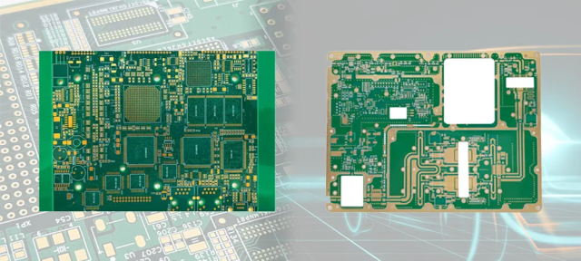
At KKPCB, we specialize in high-frequency ADAS radar PCB fabrication using premium low-loss materials like Rogers RO3003, RO3003G2, and RO4835. Our advanced manufacturing processes ensure exceptional signal integrity, tight impedance control, and full compliance with stringent automotive standards including AEC-Q100, IATF 16949, and ISO 26262 functional safety — delivering reliable, production-ready 77 GHz radar PCBs for Tier-1 suppliers and ADAS system integrators.
Why High-Frequency ADAS Radar PCB Layout Demands Special Attention

At 77 GHz, the wavelength shrinks to approximately 3.9 mm in free space (even shorter on PCB), turning every trace into a precise transmission line. Key challenges include:
- Ultra-low insertion loss to maximize detection range and resolution
- Stable dielectric constant (Dk) across temperature and frequency for consistent antenna performance
- Excellent thermal and mechanical reliability under harsh automotive conditions (-40°C to +125°C, vibration, humidity)
- Effective isolation between RF, high-speed digital, and power sections to prevent EMI and crosstalk
- Minimized glass weave effect and copper surface roughness for reduced conductor and dielectric loss
Poor ADAS PCB layout can easily result in >0.5 dB extra loss per trace or unwanted resonances, directly impacting radar system performance and safety.
Recommended Materials for 77 GHz Automotive Radar PCBs
Material selection is the foundation of successful high-frequency ADAS radar PCB design. Preferred laminates include:
- Rogers RO3003 / RO3003G2: Dk ≈ 3.00 ± 0.04, ultra-low Df ≈ 0.0010 @ 10 GHz. Glass-weave-free for superior dielectric uniformity and minimal phase variation across temperature.
- Rogers RO4835 / RO4830: Excellent long-term oxidation resistance and thermal stability for automotive reliability.
- Hybrid stack-ups combining low-loss RF layers (RO3003) with cost-effective FR-4 for digital and power sections.
These materials minimize insertion loss, provide tight Dk control, and eliminate glass weave effects that could cause resonances at 77 GHz.
Optimal Layer Stack-Up for ADAS Radar PCBs
A well-engineered stack-up is essential for ADAS radar PCB signal integrity:
- Typical 4–8 layer configuration:
- Top Layer (L1): Antenna arrays, RF front-end (MMIC, LNA, PA) with microstrip or patch structures.
- Layer 2: Solid ground plane for immediate RF return path and shielding.
- Inner layers: Controlled-impedance RF routing, high-speed digital signals, and carefully partitioned power planes.
- Bottom layers: Additional routing or ground for mechanical stability.
- Maintain symmetric stack-up to minimize warpage under thermal cycling.
- Use thin, uniform dielectrics between signal and reference layers for precise 50 Ω single-ended or 100 Ω differential impedance.
- Incorporate dense ground via stitching around RF zones for low-inductance returns and EMI suppression.
Best Practices for High-Frequency ADAS Radar PCB Layout
- Component Placement and Antenna Optimization Place RF MMICs and front-end components extremely close to antenna arrays to keep 77 GHz traces under 10 mm where possible. Spatially separate RF, digital, and power domains. Position antennas for unobstructed field of view while avoiding tall components or metal features that could distort radiation patterns.
- Transmission Line and Trace Design Treat all RF paths as controlled-impedance lines (microstrip, stripline, or CPW). Use smooth VLP/HVLP copper foils to reduce skin-effect loss. Maintain consistent trace width and spacing with 45° miters or curved bends. Keep traces short and straight to limit attenuation. Avoid via stubs at 77 GHz — employ back-drilling, blind, or buried vias when transitions are unavoidable.
- Grounding, Shielding, and EMI Control Provide continuous ground planes beneath all RF areas. Implement via fencing at intervals of ~λ/20 for effective shielding. Use guard traces, moats, or compartmental metal shields to isolate sensitive receiver circuits from noise sources.
- Thermal Management in Radar PCBs High-power MMICs and processors require robust heat dissipation. Deploy dense thermal vias, copper pours, and heatsink solutions under hot components while preserving RF performance. Balance thermal relief with signal integrity needs.
- Power Distribution and Decoupling Dedicate clean power planes with multiple low-ESR decoupling capacitors placed directly at IC pins. Isolate power domains to prevent switching noise from coupling into the RF section.
- Design for Manufacturability and Automotive Reliability Follow IPC-6018 and IPC-2252 guidelines for high-frequency boards. Ensure symmetric copper distribution and tight manufacturing tolerances (±5% impedance or better). Include test points, fiducials, and panelization features optimized for high-volume SMT assembly and AOI/X-ray inspection.
KKPCB’s Expertise in ADAS Radar PCB Manufacturing
KKPCB offers comprehensive capabilities tailored for 77 GHz automotive radar systems:
- Expert fabrication with Rogers RO3003, RO4835, and hybrid constructions
- Precision controlled impedance, laser drilling, and advanced lamination processes
- Full automotive certifications (IATF 16949) and functional safety support
- One-stop turnkey services: DFM analysis, material sourcing, PCBA, RF testing (VNA up to mmWave), and environmental verification
- Proven results delivering longer detection range, higher resolution, and superior reliability in real-world ADAS applications
Future Trends in ADAS Radar PCB Design
Next-generation ADAS radar PCBs are evolving toward wider bandwidths (>4 GHz), multi-sensor fusion, antenna-in-package integration, and higher levels of autonomy (L3+). This drives demand for finer HDI structures, embedded antennas, and advanced thermal solutions — areas where KKPCB continues to invest for future-ready manufacturing.
Ready to elevate your ADAS automotive radar PCB performance? Share your Gerber files, stack-up details, target frequency, or schematic with the KKPCB engineering team. Receive free expert DFM feedback, material recommendations, impedance modeling, thermal analysis, and rapid prototypes — helping you achieve first-pass success and accelerate time-to-market for reliable, high-performance ADAS radar systems.
