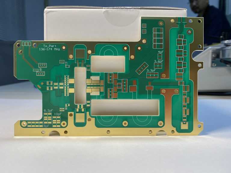
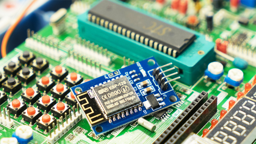
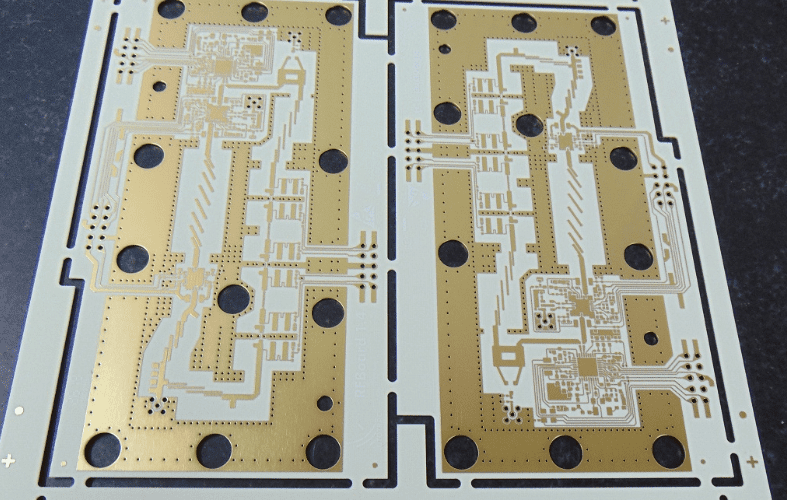
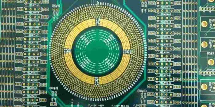
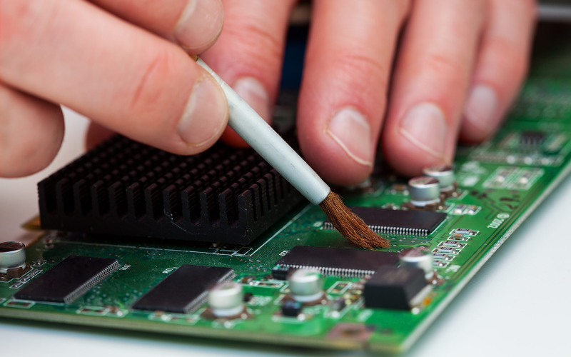
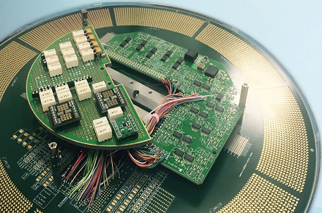
KKPCB Blog – PCB & PCBA Insights, News, and Tips - KKPCB
 

Blog

Explore the KKPCB Blog for the latest PCB manufacturing and assembly news, industry insights, expert tips, and technology trends, helping you stay informed and optimize your electronics projects.
Maximize Performance With PCB Cross-Hatching

Key Takeaways Cross-hatching significantly increases the flexibility of flex PCBs by reducing copper content. Helps maintain optimal impedance in flex PCBs without altering dielectric thickness or signal line width. Enables efficient manufacturing with reduced copper usage and improved resin adhesion. Cross-hatch PCB connector PCB cross-hatching is a technique where certain planes or large copper areas are designed...

Rigid Flex PCB Cost Optimization

Key Takeaways Rigid flex PCBs combine the challenges of rigid board and flex PCB design. The flexibility, small package size, and durability advantages of rigid-flex can be negated by the complexity, material, equipment specialities and lifecycle structural integrity challenges associated with rigid flex PCBs. OrCAD X includes functionalities and capabilities to help you overcome rigid flex PCB...

How to Check for PCB Warpage: Techniques and Methods

Key Takeaways Stress during fabrication, such as thermal expansion and contraction, imbalanced copper distribution, and improper handling, can lead to warpage. Utilize tools like feeler gauges, height gauges, contour gauges, optical profilometers, and Finite Element Method (FEM) simulations to accurately measure PCB warpage. Effective design practices using OrCAD X, such as symmetrical component placement and...

How to Create a Variable Power Supply PCB Layout

Key Takeaways Understand the purpose of each component in a variable power supply, including transformers, rectifiers, capacitors, and regulators. Learn about different topologies for variable power supplies, from discrete resistor selection to continuously variable potentiometer-based designs. Discover how OrCAD X  tools like DFM, interactive routing, constraint management, and thermal analysis can streamline the design and optimization...

Prototype PCB Design Software Essentials

Key Takeaways The competitiveness of new product introduction makes it critical to optimize your prototype design process for effectiveness and efficiency. Your prototype PCB design software should exhibit essential attributes for managing component inventory, creating schematics, designing PCBs, verifying designs, and managing data. OrCAD X delivers the essential functionality and capabilities in one program for prototype design...

Introduction to PCB Design

PCB design involves two critical stages: component layout and circuit connection wiring. The layout is the arrangement of circuit components within the PCB’s wiring area. A well-thought-out layout directly affects the ease of subsequent wiring and significantly impacts the PCB’s overall performance. In addition to meeting circuit functionality and performance requirements, a good layout considers manufacturability, inspection, and maintenance....

Electromagnetic Compatibility Design of Mobile Phone PCB

Electromagnetic compatibility (EMC) refers to the ability of electronic devices to function harmoniously in their electromagnetic environment without causing or being affected by electromagnetic interference (EMI). The goal of EMC design is to enable electronic devices to resist external interference while minimizing the electromagnetic interference they emit to surrounding devices. 1. Selecting the Right Wire Width Minimizing inductance...

The Five Golden Rules of PCB Design

Printed Circuit Boards (PCBs) are the backbone of electronic circuits, organizing and supporting all circuit components. Effective PCB design not only assembles components efficiently but also prevents errors caused by manual wiring. This article highlights five essential PCB design principles that enhance power supply design and improve overall performance. 1. Maintain a Logical Direction Segregate Signals: Group inputs/outputs,...

10 Key Steps to Ensure Signal Integrity (SI) in PCB Design

Introduction: Addressing signal integrity (SI) issues early in the PCB design process can streamline the design and eliminate the need for corrective termination devices later. Here, we outline critical steps to maintain signal integrity, from planning through testing. 1. Preparation Before Design Begin by defining your SI requirements and design strategy. Early-stage planning will guide component selection,...

High-Frequency Circuit Design Solution Based on RT/duroid® 6010.2LM Material for Miniaturization

Solution Refinement and Layout: As the demand for smaller and more portable electronic devices continues to grow, the design of RF and microwave circuits is shifting towards more compact and efficient solutions. In high-frequency circuit design, the choice of PCB materials is crucial for determining circuit size, performance, and signal propagation characteristics. RT/duroid® 6010.2LM, a high-frequency...