
The Role of Package Test PCB in Semiconductor Testing
In semiconductor testing, measurement accuracy, test repeatability, and production efficiency are critical factors affecting IC quality and manufacturing cost.
A Package Test PCB is a specialized interface board used in Automated Test Equipment (ATE) systems to evaluate packaged semiconductor devices after assembly. It provides the electrical and mechanical connection between test sockets, probe interfaces, and the Device Under Test (DUT), ensuring stable signal transmission and accurate measurement results.
As advanced ICs continue to evolve toward smaller package sizes, higher I/O density, faster signal speeds, and more complex mixed-signal architectures, Package Test PCBs must achieve excellent electrical performance, mechanical precision, and manufacturing consistency.
What Makes Package Test PCB Critical for IC Testing?
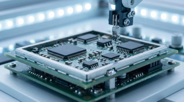
Unlike conventional functional PCBs, Package Test PCBs are designed specifically for semiconductor test environments where:
- Electrical accuracy is more important than product functionality
- High-density interconnections are required
- Signal integrity must be maintained across multiple test channels
- Mechanical alignment must remain stable during repeated testing cycles
Any inconsistency in PCB performance may affect test accuracy, increase false failures, and reduce semiconductor production efficiency.
Key Design Considerations for Package Test PCBs
1. High-Density Routing and Fine-Pitch Interface Design
Modern IC packages such as BGA, QFN, LGA, CSP, and SiP require highly dense interconnections between the device and test system.
Major challenges include:
- Limited routing space
- High pin-count fanout requirements
- Fine-pitch pad structures
- Via reliability in dense layouts
To address these challenges, Package Test PCBs often utilize:
- HDI multilayer structures
- Microvias and blind/buried vias
- Fine-line routing technology
- Optimized layer stack-up design
These technologies enable reliable signal access while maintaining electrical performance.
2. Signal Integrity and Controlled Impedance Requirements
With increasing IC operating speeds, signal quality has become one of the most important factors in Package Test PCB design.
Potential issues include:
- Impedance mismatch
- Signal reflection
- Crosstalk
- Insertion loss
- Timing deviation
Reliable designs require:
- Controlled impedance routing
- Accurate stack-up planning
- Matched signal lengths
- Proper reference plane structures
Maintaining stable signal behavior helps ensure accurate semiconductor measurements.
3. Mechanical Precision and Socket Compatibility
Package Test PCBs frequently operate with test sockets or probe interfaces that require precise mechanical alignment.
Important considerations include:
- PCB flatness control
- Pad position accuracy
- Dimensional stability
- Connector and socket reinforcement
Since test boards may experience thousands of insertion and removal cycles, mechanical reliability directly impacts contact consistency and test uptime.
4. Power Integrity and Grounding Performance
Advanced IC testing often involves high-speed switching and dynamic power requirements.
Poor power distribution can result in:
- Voltage fluctuations
- Ground noise
- Measurement instability
- Incorrect test results
Effective Package Test PCB designs incorporate:
- Optimized power distribution networks (PDN)
- Low-impedance power planes
- Proper decoupling capacitor placement
- Solid grounding structures
These approaches help maintain stable test conditions for digital, analog, RF, and mixed-signal devices.
5. Thermal Reliability and Material Selection
During continuous testing, Package Test PCBs experience thermal cycling and mechanical stress.
Common reliability considerations include:
- High-Tg materials for thermal stability
- Low-loss materials for high-frequency applications
- Controlled thermal expansion
- Warpage prevention
Proper material selection ensures consistent electrical performance throughout extended testing periods.
Manufacturing Requirements for High-Performance Package Test PCBs
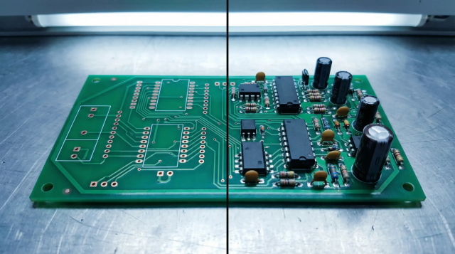
Producing reliable Package Test PCBs requires strict manufacturing control, including:
HDI and High-Density Fabrication
- Microvia reliability
- Fine-line processing
- Accurate layer registration
Electrical Performance Control
- Controlled impedance verification
- Signal performance testing
- Stable dielectric thickness
Mechanical Precision
- Tight dimensional control
- PCB flatness management
- Consistent connector interface quality
Production Flexibility
- Prototype validation
- Small-batch production
- Volume manufacturing support
Manufacturing consistency is essential to ensure repeatable semiconductor test performance.
Applications of Package Test PCBs
Package Test PCBs are widely used in:
- Logic and processor IC testing
- Memory device validation
- RF and mmWave semiconductor testing
- Automotive semiconductor quality inspection
- Industrial and high-reliability electronic testing
Each application requires stable electrical performance, precise mechanical interfaces, and reliable test repeatability.
Why Package Test PCB Quality Directly Impacts Test Results
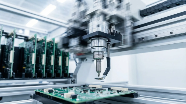
Poor-quality Package Test PCBs may lead to:
- Unstable electrical contact
- Signal degradation
- Increased false failures
- Reduced test efficiency
- Higher ATE maintenance requirements
A high-quality Package Test PCB helps semiconductor manufacturers achieve:
- More accurate measurements
- Improved test repeatability
- Higher production efficiency
- Reduced testing risks
Conclusion: Enabling Reliable Semiconductor Testing Through Advanced Package Test PCB Design
Package Test PCBs play a critical role in semiconductor validation and production testing by providing accurate electrical connections, stable signal transmission, and reliable mechanical performance.
As IC technologies continue advancing toward higher density and faster speeds, Package Test PCB design and manufacturing capabilities become increasingly important.
Working with an experienced Package Test PCB manufacturer with strong capabilities in HDI fabrication, controlled impedance, and precision manufacturing helps ensure reliable test performance and long-term production stability.





