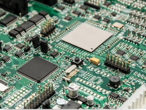
kkpcba-Cindy - KKPCB - Page 45 of 73
 
HomeAuthor

kkpcba-Cindy - KKPCB - Page 45 of 73

Classification and Parameters of PCB Board Materials: Comprehensive Guide

Overview of PCB Materials Printed Circuit Boards (PCBs) are fabricated using various materials to meet specific performance and application requirements. In China, PCB copper-clad laminates (CCLs) are extensively used, and they can be categorized by base materials, resin adhesives, flame retardancy, and performance levels. Types of Copper-Clad Laminates (CCLs) 1. Classification by Reinforcement Material Paper-based materials: Typically used for low-cost...

High-Speed PCB Design Guide XI: How to Improve Testability

As electronic devices become increasingly miniaturized, advancements in component and wiring technologies have created new challenges for production testing. Highly integrated ICs, smaller insulation spacings, and limited access to circuit nodes have made traditional testing methods insufficient. To address these challenges, a design-for-testability (DFT) approach is essential to reduce testing costs and enhance production efficiency. This...

High-Speed PCB Design Guide 9: Mastering IC Packaging Characteristics

Electromagnetic interference (EMI) control is critical in high-speed PCB design, and one often-overlooked aspect is the influence of integrated circuit (IC) packaging. Incorporating decoupling capacitors within the IC package can effectively reduce EMI and enhance signal integrity. This guide delves into the role of IC packaging in EMI suppression, exploring the root causes of EMI, key IC package design...

High-Speed PCB Design Guide 8: PCB Reliability Design

Printed circuit boards (PCBs) remain the backbone of electronic assembly across various systems. Even with perfectly designed schematics, poor PCB design can significantly compromise reliability. For instance, closely spaced thin parallel lines on a PCB can cause signal waveform delays and reflected noise at transmission line terminals. This guide outlines essential considerations for designing reliable PCBs. 1. Ground Wire...

High-Speed PCB Design Guide 7: Reducing RF Effects in PCB Interconnection Design

PCB interconnections can be categorized into three main types: chip-to-PCB, interconnections within the PCB, and PCB-to-external devices. High-frequency PCB designs require addressing RF effects at these interconnection points to ensure optimal performance. This guide covers techniques for minimizing RF interference, crosstalk, and return loss across these interconnection types. The Impact of High-Frequency Signals on PCB Design As...

High-speed PCB design guide 6: Application technology of PowerPCB in PCB design

PCBs are critical in electronic devices, ensuring electrical connections between components. With increasing circuit density, proper PCB design techniques are essential to ensure reliability and reduce interference. General PCB Design Principles Wiring Guidelines: Avoid Parallel Wires: Insert ground wires between input/output wires to reduce feedback. Conductor Width: Choose widths based on current requirements (e.g., 1.5mm width for 2A current). Conductor Bends: Use...

High-Speed PCB Design Guide 5: Noise Reduction Technology for DSP Systems

With the rise of high-speed DSPs (Digital Signal Processors) and peripherals, managing Electromagnetic Interference (EMI) has become a crucial aspect of design. In the past, issues of emission and interference were broadly referred to as EMI or RFI (Radio Frequency Interference). Today, these are part of a more nuanced area: Electromagnetic Compatibility (EMC), which encompasses both emission control...

High-Speed PCB Design Guide 3: Signal Isolation Technology

Signal isolation is critical for transmitting digital or analog signals without direct current flow between the transmitter and receiver. This technology prevents ground loops, mitigates noise, and ensures operator safety in systems with varying ground potentials. Here’s a detailed breakdown of signal isolation technologies, their applications, and design considerations. 1. Signal Isolation Basics Purpose of...

High-Speed PCB Design Guide 2: Avoiding Pitfalls in Mixed-Signal Systems

Designing mixed-signal systems requires attention to placement, trace layout, and protection elements. Today’s SOCs necessitate expertise in digital, analog, and thermal design, pushing system designers to mitigate common pitfalls such as noise, ground bounce, and latch-up. 1. Challenges in Mixed-Signal Systems High-Speed Trends The drive for higher performance in systems like PCs and servers has...

High-Speed PCB Design Guide (Part 1): Basic Concepts of PCB

When designing high-speed PCBs, understanding the core concepts is crucial for ensuring efficiency and functionality. This guide introduces key elements such as layers, vias, pads, and more to help beginners and professionals alike. 1. The Concept of “Layer” PCB layers represent the actual copper foil layers within the board material, unlike virtual layers in software. Modern...