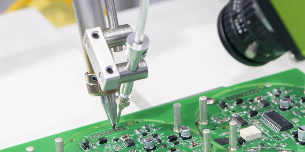
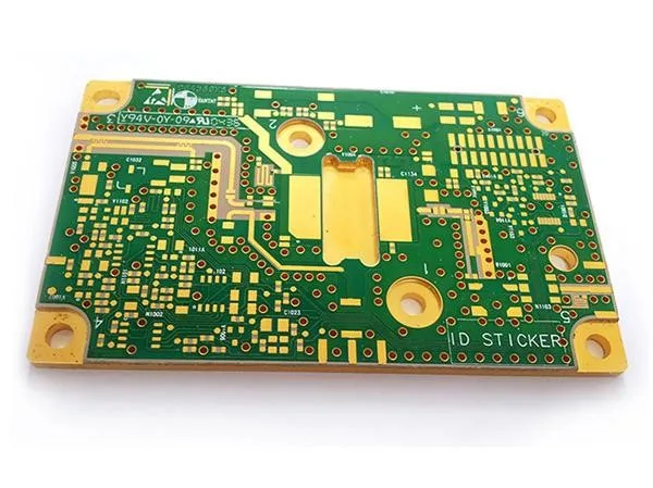
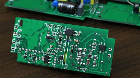
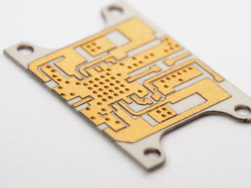
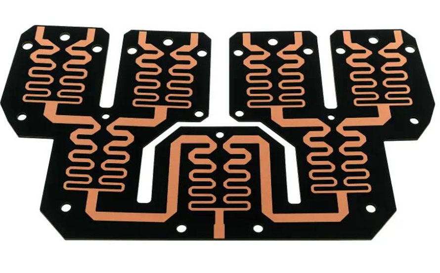
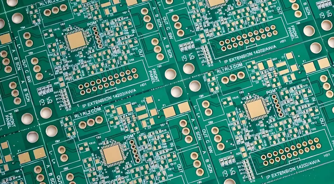
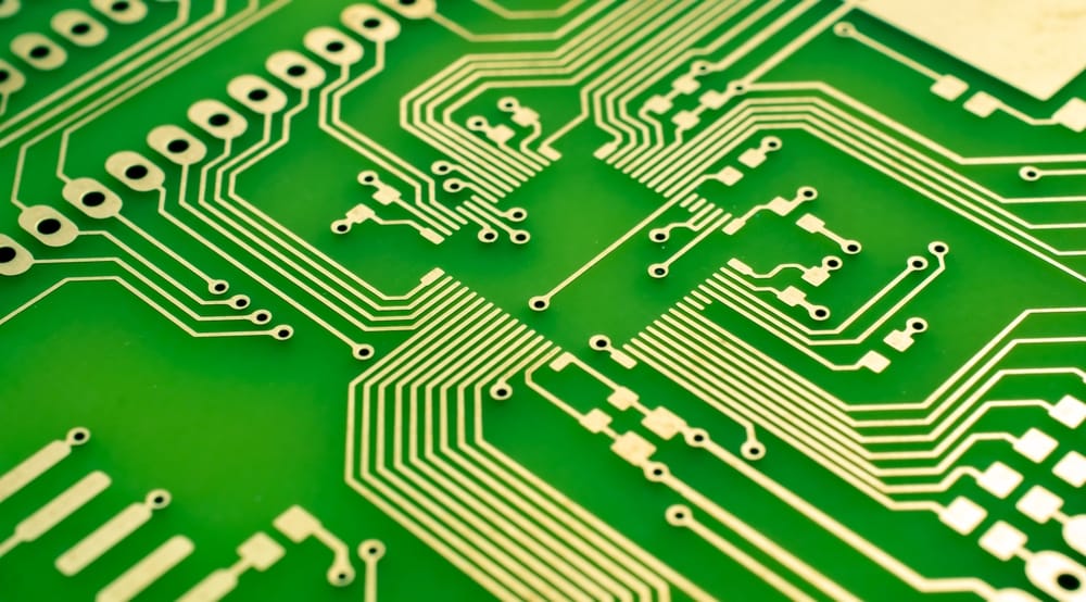
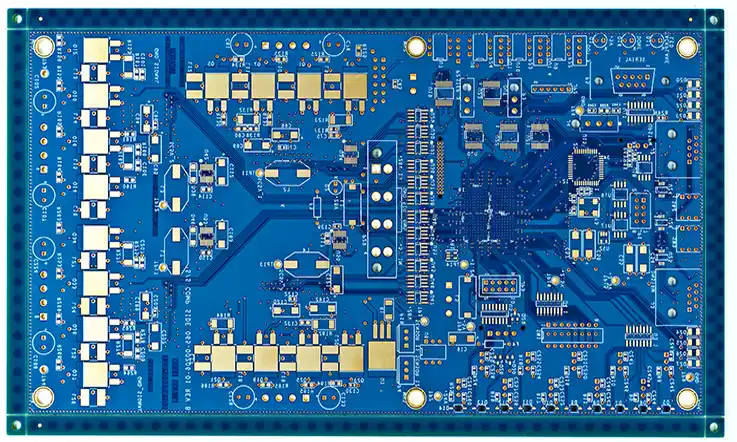
What is a Megtron PCB? A Megtron PCB is a printed circuit board built using Megtron high-frequency laminates, developed to provide low dielectric loss (Df), stable dielectric constant (Dk), and excellent thermal performance for high-speed and high-frequency electronics. Megtron laminates are commonly used in: High-speed communication devices RF and microwave circuits Gigabit and multi-gigabit data...
HomeAuthor
kkpcb04 - KKPCB - Page 4 of 96
What is a Logic Test PCB? A Logic Test PCB is a printed circuit board specifically created for testing and verifying digital circuits, logic gates, microcontrollers, and complex integrated circuits (ICs). Unlike standard production PCBs, logic test boards are engineered to facilitate troubleshooting, functional testing, and rapid prototyping of digital electronics. Logic test PCBs are...
What is a Taconic PCB? A Taconic PCB is a printed circuit board made using Taconic high-frequency laminates, engineered for minimal signal loss, stable dielectric constant (Dk), and superior thermal performance in RF, microwave, and high-speed digital applications. Taconic materials, such as TLY, RF-35, and CER-10 series, are widely used where conventional FR-4 or standard...
What is a High Frequency Laminate PCB? A High Frequency Laminate PCB is a printed circuit board built with specialized substrate materials optimized for low dielectric loss (Df), stable dielectric constant (Dk), and high thermal performance at high frequencies. Unlike standard FR-4, high frequency laminates maintain signal integrity in RF, microwave, and high-speed digital applications,...
What is a Ceramic PCB? A Ceramic PCB is a printed circuit board built using ceramic substrates like alumina (Al₂O₃), aluminum nitride (AlN), or silicon nitride (Si₃N₄) instead of standard FR-4 or PTFE materials. These substrates are thermally conductive, electrically insulating, and mechanically robust, making them ideal for high-power electronics and RF/microwave applications. Ceramic PCBs...
What is a PTFE PCB? A PTFE PCB is a printed circuit board built using polytetrafluoroethylene (PTFE) as the substrate. PTFE is a high-performance polymer renowned for its extremely low dielectric loss (Df), consistent dielectric constant (Dk), and high thermal stability. These characteristics make PTFE PCBs ideal for applications where high-frequency signal integrity and minimal...
What is a Rogers PCB? A Rogers PCB is a printed circuit board manufactured using high-performance laminates developed by Rogers Corporation, designed specifically for high-frequency, RF, and microwave applications. Unlike standard FR-4 materials, Rogers substrates offer low dielectric loss (Df), stable dielectric constant (Dk), and superior thermal performance, making them ideal for high-speed and high-frequency...
What is an RF Trace PCB? An RF Trace PCB is a printed circuit board specifically designed to handle high-frequency radio frequency (RF) signals, typically ranging from MHz to GHz and even mmWave frequencies. Unlike standard PCB traces, RF traces must be carefully engineered to behave as controlled transmission lines, ensuring signals propagate with minimal...
What is a Fine Line PCB? A Fine Line PCB is a printed circuit board designed with extremely narrow trace widths and spacing, typically below 100 microns. These PCBs are essential for high-density electronic designs where space is limited and performance requirements are demanding. Fine line technology is widely used in applications that require compact...
What is a High Current PCB? A High Current PCB is a printed circuit board designed to carry large currents—often several amps or more—while maintaining electrical performance and thermal stability. Unlike standard PCBs, high current boards require thicker copper, optimized trace widths, and precise thermal management to prevent overheating, voltage drop, and potential damage. High...

