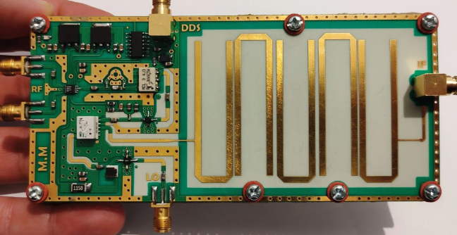
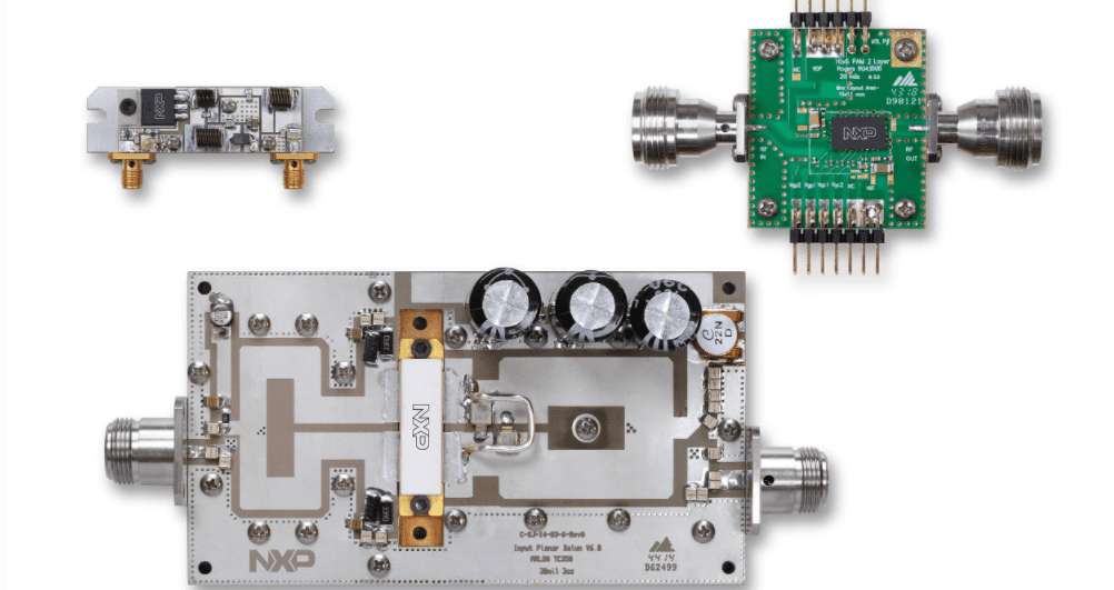
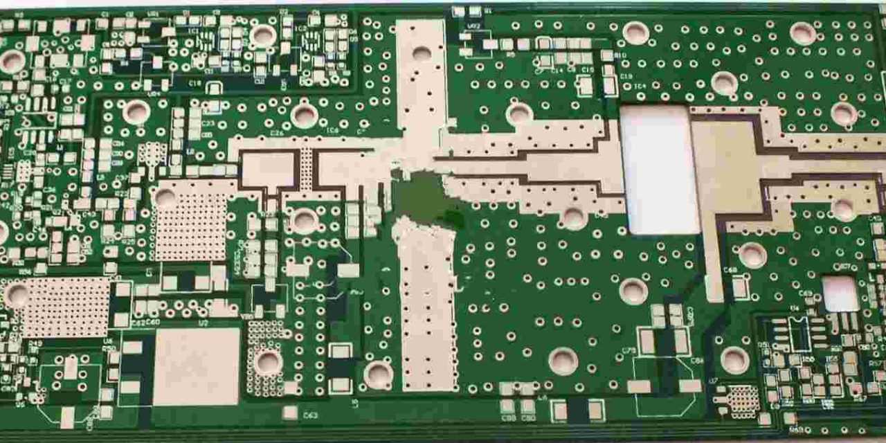
signal integrity PCB - KKPCB
 
HomeTag

signal integrity PCB - KKPCB

Controlled Impedance PCB Engineering for High-Speed Digital and High-Frequency RF Applications

A Controlled Impedance PCB is a critical foundation for modern high-speed digital systems and high-frequency RF applications. As signal rise times shrink and operating frequencies extend into multi-GHz ranges, PCB interconnects must behave as predictable transmission lines rather than simple copper connections. Controlled Impedance PCB design ensures signal integrity, phase stability, and EMI compliance across...

Enable Ultra-High Interconnect Density and Signal Integrity with Advanced High Layer Count PCB Architectures

High Layer Count PCB: The Backbone of Complex Electronic Systems A High Layer Count PCB refers to a multilayer printed circuit board typically featuring 16 layers, 24 layers, 32 layers, or more, designed to support complex signal routing, dense interconnections, and advanced power distribution. As electronic systems continue to integrate higher data rates, tighter form...

Enhance Routing Density and Signal Integrity with Buried Via PCB Architectures for High-Density Electronic Systems

Buried Via PCB: Enabling High-Density Interconnection Beyond Conventional Multilayer Boards A Buried Via PCB is a multilayer printed circuit board in which vias connect only internal layers and do not extend to the outer layers. Unlike through-hole vias, buried vias are completely embedded within the PCB stackup, enabling higher routing density, improved signal integrity, and...

Enable Ultra-Complex Routing and Signal Integrity with High Layer Count PCB Architectures for Advanced Electronic Systems

High Layer Count PCB: The Backbone of Ultra-Complex Electronic Integration A High Layer Count PCB refers to a multilayer printed circuit board typically exceeding 12 layers and extending to 20, 30, or even 60+ layers for advanced electronic systems. High layer count PCB designs are essential for applications requiring dense routing, high-speed signal transmission, controlled...

Optimize High-Frequency Signal Integrity and Power Efficiency with Low Dissipation Factor PCB Materials

Why Low Dissipation Factor PCB Matters in High-Frequency Electronics As electronic systems evolve toward higher frequencies, faster data rates, and tighter power budgets, signal loss within the PCB itself becomes a dominant performance constraint. In RF, microwave, mmWave, high-speed digital, and satellite communication systems, even minor dielectric losses can accumulate across long signal paths, directly...

High Speed PCB Engineering for Signal Integrity, Power Integrity, and Ultra-Low-Latency Electronic Systems

As modern electronics become faster, more compact, and more data-intensive, the High Speed PCB has evolved into a critical engineering platform for communication systems, servers, AI accelerators, radar units, embedded computing modules, and advanced industrial electronics. A well-engineered High Speed PCB ensures clean signal transmission, stable power behavior, and low-jitter operation across multi-gigabit channels. High-speed...

Advanced Robotics PCB Design: Optimizing Signal Integrity, Power Distribution, and Sensor Integration for Industrial Automation

Modern industrial automation, autonomous robots, and collaborative robotic systems depend heavily on Robotics PCBs as the central electronic platform for control, sensing, and communication. Engineers designing Robotics PCBs face unique challenges: ensuring low-latency signal transmission, maintaining power stability for high-current actuators, integrating a diverse set of sensors, and protecting sensitive electronics from electromagnetic interference. 1....

Engineering Low Dissipation Factor PCBs for High-Frequency and RF Performance

1. Engineering Context  As electronic systems push into higher frequencies—5G, mmWave sensing, radar, satellite communication, and precision instrumentation—the dissipation factor (Df) of PCB materials has become a primary performance determinant.A Low Dissipation Factor PCB minimizes dielectric loss, preserves signal integrity, and ensures stable operation at frequencies where traditional FR-4 rapidly degrades. Low Df PCBs bridge...

Optimize High-Frequency Signal Integrity and Thermal Stability with TLY-5 PCB Laminates for 5G RF Front-End Modules

As 5G RF front-end modules push into sub-6 GHz and mmWave bands, PCB materials must deliver extreme electrical precision, low-loss propagation, and predictable thermal behavior. TLY-5 PCB laminates, based on PTFE composites engineered with ultra-low dielectric constant (Dk ≈ 2.17) and low dissipation factor (Df ≈ 0.0009), have emerged as one of the most reliable...

Boost Design Accuracy and Signal Integrity Using High-Precision PCB Prototype Fabrication Technologies

High-precision PCB prototype fabrication has become the backbone of modern electronics development. As product cycles shrink and system complexity rises—spanning RF modules, high-speed digital interfaces, IoT sensors, EV power systems, and aerospace electronics—the demand for PCB prototype accuracy, signal integrity stability, and manufacturing predictability has never been higher. A high-reliability prototype is not “just a...