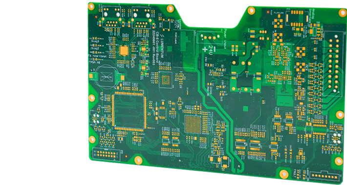
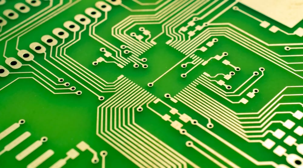
Signal Integrity - KKPCB
 
HomeTag

Signal Integrity - KKPCB

Impedance Control on PCBs: Why It Matters for High-Speed, RF, and High-Frequency Circuit Design

As electronic devices continue to evolve toward higher speeds, greater bandwidth, and higher operating frequencies, impedance control on PCBs has become a critical requirement rather than an optional design consideration. In high-speed PCB, RF PCB, and high-frequency circuit design, improper impedance control can lead to signal degradation, EMI issues, and overall system instability. This article...

Key Manufacturing Factors That Affect Controlled Impedance PCB Accuracy

Key Manufacturing Factors That Affect Controlled Impedance PCB Accuracy In today’s high-speed electronics market, Controlled Impedance PCB manufacturing has become a fundamental requirement for ensuring excellent signal integrity and stable electrical performance. As operating frequencies and data transmission speeds continue to rise, even minor impedance deviations in a controlled impedance PCB can result in signal...

Building Reliable High-Speed Electronics with Controlled Impedance PCB Architectures

Introduction: Why Controlled Impedance Defines High-Speed Reliability As high-speed electronics push into multi-gigabit data rates and high-frequency RF domains, signal behavior is no longer dominated by logic thresholds—it is governed by transmission line physics. In these systems, every PCB trace behaves as a controlled impedance structure, and any deviation can introduce reflections, timing skew, and...

Balancing Electrical Performance and Manufacturability in Buried Via PCB Structures

As electronic systems continue to evolve toward higher speeds, greater functionality, and reduced form factors, Buried Via PCB structures have become a critical enabler for advanced multilayer designs. By allowing interlayer connections without penetrating the outer layers, buried vias unlock higher routing density, improved signal integrity, and enhanced EMI control. However, these electrical advantages must...

High-Speed PCB Design & Manufacturing Guide | Signal Integrity, Materials & KKPCB Engineering Capabilities

High-Speed PCB: Engineering Principles, Core Challenges & KKPCB Capabilities High-Speed PCB technology is at the center of every modern data-intensive system—from 5G infrastructure and AI servers to autonomous machines and aerospace communication modules. As signal frequencies climb beyond 3 GHz, 10 GHz, even 28–56 Gbps, traditional PCB design rules become insufficient. High-speed PCB engineering demands...

Engineering High Speed PCB for Signal Integrity, Low-Loss Routing, and Next-Generation Data Transmission

As digital systems move toward higher data rates, smaller form factors, and lower power consumption, the demand for High Speed PCB solutions continues to accelerate. From 10–112 Gbps SerDes links to DDR4/DDR5 memory buses and advanced communication modules, a High Speed PCB must deliver loss control, impedance stability, and electromagnetic reliability in increasingly complex environments....

High Speed PCB Engineering Strategies for Ultra-Reliable, High-Bandwidth, Next-Generation Electronic Systems

A High Speed PCB is no longer a specialty board reserved for telecom giants—it has become the core platform for every high-bandwidth, low-latency, high-frequency electronic architecture. Whether powering 56G/112G SerDes, PCIe 5.0/6.0 interconnects, next-generation routers, AI accelerator hardware, or advanced radar/5G infrastructure, the High Speed PCB defines the system’s ultimate signal integrity, timing accuracy, power...

Shorten R&D Cycles with Cost-Optimized, High-Reliability PCB Prototype Solutions for Rapid Electronics Development

Rapid electronics development has entered an era where design cycles are measured not in months but in weeks. From IoT edge devices to next-generation communication modules and automotive sensing platforms, engineers must iterate faster while maintaining electrical performance, manufacturability, and long-term reliability. PCB prototypes sit at the heart of this acceleration. When engineered correctly, they...

Enhance Signal Accuracy and Low-Noise Stability with High Frequency Sensor PCB Platforms for Industrial IoT Detection Systems

Industrial IoT detection systems rely on a dense network of sensors for accurate monitoring of environmental parameters, machinery status, and process analytics. High frequency sensor PCBs must maintain low insertion loss, high signal-to-noise ratio, and phase-stable routing across multiple sensor channels to ensure reliable data acquisition. High frequency sensor PCB laminates (Dk = 3.2 ±...

Maximize RF Channel Integrity and Minimize Signal Loss with Blind Via PCB Architectures for High-Speed Communication Modules

High-speed communication modules in 5G, satellite transceivers, and high-frequency computing systems demand extreme precision in signal routing and interconnect integrity. As layer density increases and modules become more compact, traditional through-hole vias introduce unwanted parasitic effects, signal reflection, and EMI interference, compromising both channel fidelity and system performance. Blind via PCB technology enables selective inter-layer...