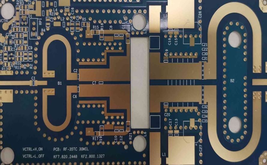
phase-stable PCB - KKPCB
 
HomeTag

phase-stable PCB - KKPCB

Reduce Insertion Loss and Enhance Power Efficiency Using Low Loss PCB Designs for Satellite Communication Payloads

Satellite communication payloads demand high-frequency RF stability, minimal insertion loss, and optimized power efficiency across densely packed multilayer PCBs. Signal integrity degradation, EMI coupling, or thermal hotspots can compromise link margin, telemetry accuracy, and antenna performance. Low loss PCB materials, such as ceramic-reinforced laminates or PTFE-based RF substrates, provide stable dielectric constant (Dk) and low...

Optimize Phase-Stable High-Frequency Routing with Blind Via PCB Architectures in Compact Satellite Communication Payloads

Compact satellite communication payloads require precise, phase-stable RF routing to maintain signal fidelity and low insertion loss across high-frequency channels. The limited space and high-density requirements make blind via architectures essential for multilayer PCBs, enabling signal interconnects without penetrating all layers, reducing parasitic capacitance, and controlling crosstalk. Blind via PCBs allow compact routing of RF...

Improve Multi-Gigabit Transmission and Low-Loss Routing Through Impedance Controlled PCB Engineering for Data Center Switches

Modern data center switches demand high-speed, multi-gigabit transmission across densely packed PCB layers. Maintaining low insertion loss, tight impedance control, and minimal crosstalk is critical to guarantee reliable signal integrity, reduce latency, and preserve network throughput. Impedance-controlled PCB architectures provide predictable high-frequency performance for differential pair routing and dense multilayer stackups. KKPCB leverages precision lamination,...

Optimize Thermal Resilience and Multi-Layer Signal Fidelity with Megtron 7 PCB Stackups in High-Performance Computing Modules

High-performance computing modules in data centers, AI accelerators, and HPC servers operate with dense multi-layer interconnects and high-frequency signaling. Signal degradation, thermal hotspots, and impedance drift can severely impact throughput and reliability. Megtron 7 PCB laminates offer low-loss dielectric properties, tight Dk/Df tolerances, and high thermal conductivity, enabling reliable high-speed signal transmission in complex multi-layer...

Achieve Ultra-Stable Dk/Df and Low-Loss Performance with RO4835 PCB Architectures for High-Density 5G Massive-MIMO Radio Units

Next-generation 5G massive-MIMO radio units require high-density PCB designs that maintain ultra-consistent dielectric constant (Dk) and dissipation factor (Df) across all layers. Any variation in Dk/Df can lead to impedance mismatches, phase errors, and RF signal degradation, negatively affecting beamforming accuracy and spectral efficiency. RO4835 PCB laminates (Dk = 3.48 ± 0.03, Df = 0.0037...

Enhance Signal Accuracy and Low-Noise Stability with High Frequency Sensor PCB Platforms for Industrial IoT Detection Systems

Industrial IoT detection systems rely on a dense network of sensors for accurate monitoring of environmental parameters, machinery status, and process analytics. High frequency sensor PCBs must maintain low insertion loss, high signal-to-noise ratio, and phase-stable routing across multiple sensor channels to ensure reliable data acquisition. High frequency sensor PCB laminates (Dk = 3.2 ±...

Enhance Thermal Management and Low-Loss Transmission with RO4350B PCB Stackups for 5G mmWave Base Station Units

5G mmWave base station modules require high-frequency RF interconnects that maintain low insertion loss, phase stability, and impedance accuracy under high power and dense component placement. Thermal hotspots and EMI in multilayer architectures can severely degrade link performance and reduce overall throughput. RO4350B PCB laminates (Dk = 3.48 ± 0.02, Df = 0.0037 @10 GHz)...

Maximize RF Channel Integrity and Minimize Signal Loss with Blind Via PCB Architectures for High-Speed Communication Modules

High-speed communication modules in 5G, satellite transceivers, and high-frequency computing systems demand extreme precision in signal routing and interconnect integrity. As layer density increases and modules become more compact, traditional through-hole vias introduce unwanted parasitic effects, signal reflection, and EMI interference, compromising both channel fidelity and system performance. Blind via PCB technology enables selective inter-layer...

Extend High-Temperature RF Reliability and Maintain Ultra-Tight Impedance Stability Using Multilayer HF PCB Architectures for Harsh-Environment IoT Gateways

Harsh-environment IoT gateways—used in industrial automation, outdoor base stations, energy systems, mining networks, and smart transportation infrastructure—operate under extreme thermal stress and wideband RF loading. These platforms demand stable impedance, low-loss transmission, and high-temperature RF reliability to maintain continuous connectivity across Sub-6 GHz, C-Band, and mmWave IoT communication channels. Multilayer HF PCB architectures, built with...

Extend Thermal Endurance and RF Power Efficiency with RO4835 PCB Substrates in High-Density Microwave Amplifier Designs

High-density microwave amplifiers, widely used in radar, satellite communication, and 5G mmWave systems, operate under intense thermal stress and high RF power. Maintaining ultra-low insertion loss, precise phase stability, and tight impedance control is critical to ensure amplifier efficiency, signal fidelity, and overall system reliability. RO4835 PCB laminates (Dk = 3.48 ± 0.03, Df =...