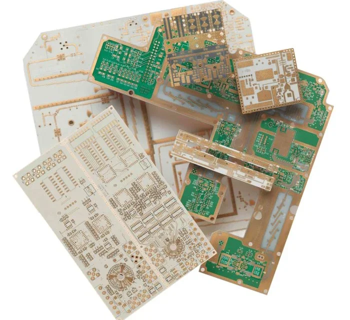
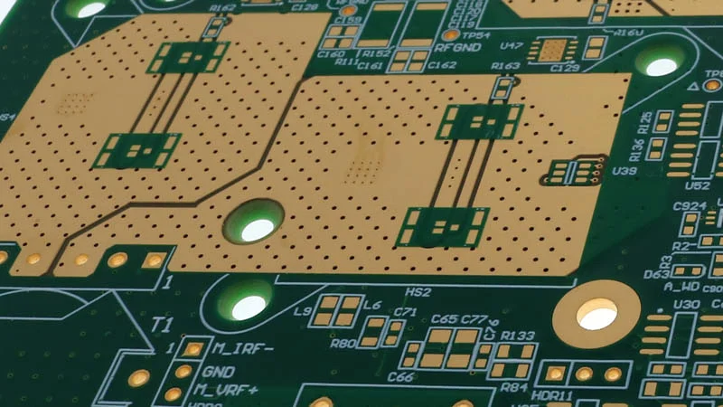
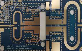
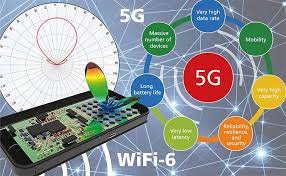
low-loss PCB materials - KKPCB
 
HomeTag

low-loss PCB materials - KKPCB

High Frequency Test PCB Design and Manufacturing for Accurate RF and Microwave Measurements

In RF, microwave, and high-speed electronics testing, measurement accuracy depends not only on instruments but also on the quality of the test interface. A High Frequency Test PCB acts as the electrical bridge between the device under test and the measurement system, making its design and fabrication critical to reliable results. Unlike standard production PCBs,...

Engineering Low Dissipation Factor PCBs for High-Frequency and RF Performance

1. Engineering Context  As electronic systems push into higher frequencies—5G, mmWave sensing, radar, satellite communication, and precision instrumentation—the dissipation factor (Df) of PCB materials has become a primary performance determinant.A Low Dissipation Factor PCB minimizes dielectric loss, preserves signal integrity, and ensures stable operation at frequencies where traditional FR-4 rapidly degrades. Low Df PCBs bridge...

Achieve Ultra-Flat Phase Response and Coherent Wideband Propagation Through Rogers 5880 PCB Laminates in High-Q RF Filters

High-Q RF filters operating in microwave, mmWave, radar, and satellite communication systems demand exceptionally stable phase behavior and predictable wideband propagation. Rogers 5880 PCB laminates have become a preferred high-frequency substrate because their ultra-low dielectric constant (Dk 2.20) and extremely low dissipation factor (Df 0.0009) enable ultra-flat phase response, low-loss signal transmission, and coherent filter...

Boost Design Accuracy and Signal Integrity Using High-Precision PCB Prototype Fabrication Technologies

High-precision PCB prototype fabrication has become the backbone of modern electronics development. As product cycles shrink and system complexity rises—spanning RF modules, high-speed digital interfaces, IoT sensors, EV power systems, and aerospace electronics—the demand for PCB prototype accuracy, signal integrity stability, and manufacturing predictability has never been higher. A high-reliability prototype is not “just a...

Achieve Phase-Stable Multi-Gigabit Routing with Low Loss PCB Stackups for High-Speed Data Center Networks

Modern data center networks depend on multi-gigabit signal transmission, low-latency switching, and phase-coherent high-speed channels. As switching fabrics migrate from 25G/40G toward 100G/200G/400G architectures, even micro-scale distortions in dielectric properties or copper structures can degrade eye diagrams, reduce SNR, and trigger packet loss.This is why Low Loss PCB stackups—built with engineered dielectric materials and ultra-controlled...

mmWave Module PCB Engineering: Material Precision, RF Loss Control, and Manufacturing Realities

Next-generation RF transceivers—whether for 5G mmWave, SATCOM terminals, phased-array antennas, or short-range high-bandwidth links—place brutal demands on PCB materials. To maintain ultra-low insertion loss, wideband consistency, stable phase response, and clean radiation efficiency, mmWave module PCB materials must deliver precision alignment, ultra-low dielectric loss, tight Dk control, and minimal copper roughness across every layer. In...

Maximize High-Frequency Signal Integrity with Low Loss PCB Laminates in 5G mmWave Antenna Systems

High-frequency signal integrity is the defining performance factor in modern 5G mmWave antenna systems, where routing density, insertion loss, and phase stability determine overall RF efficiency. As 5G architectures transition to 26–29 GHz, 37–40 GHz, and 60 GHz mmWave bands, the electrical behavior of the Low Loss PCB stackup becomes just as important as the...

Optimize Thermal Performance and EMI Suppression in High-Density RF Modules with Low Loss PCB Materials

High-density RF modules used in 5G radios, SATCOM terminals, phased-array beamformers, and mmWave front-end units are increasingly constrained by thermal stress, EMI coupling, and insertion loss. As operating frequencies push beyond 10–40 GHz, traditional FR-4 structures can no longer maintain stable impedance, consistent dielectric behavior, or low-loss routing. This is where Low Loss PCB materials—such...

Improve Wideband Isolation and EMI Suppression Using Engineered 5G Router PCB Layouts for CPE Systems

Customer-Premises Equipment (CPE) sits at the frontline of the 5G access network. Unlike traditional routers, a 5G CPE must simultaneously maintain wideband RF isolation, suppress broadband EMI, and stabilize the 2.4 GHz / 5 GHz / 6 GHz multi-band wireless channels while handling dense digital switching activity. At these frequencies, the PCB layout is no...

Optimize Differential Pair Accuracy and Reduce Crosstalk Using Impedance Controlled PCB Laminates in Automotive ADAS Radar Units

Automotive ADAS radar systems are now operating at higher frequencies, tighter channel spacing, and more aggressive signal-processing thresholds than ever. Under these conditions, the performance of an Impedance Controlled PCB becomes a dominant factor shaping radar detection accuracy, phase stability, and immunity to signal degradation. Engineering teams focusing on 77–79 GHz radar modules increasingly recognize...