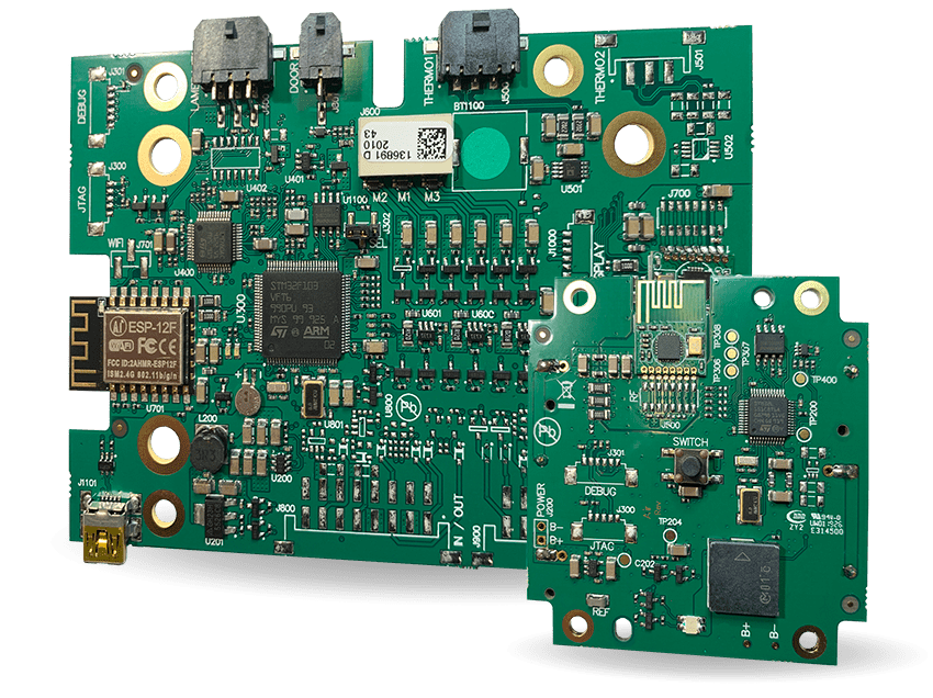
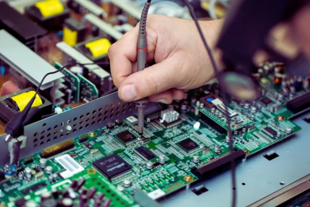
Load Board PCB - KKPCB
 
HomeTag

Load Board PCB - KKPCB

Mixed Signal IC Test PCB for High-Precision Semiconductor Testing

What Is a Mixed Signal IC Test PCB? A Mixed Signal IC Test PCB is a specialized printed circuit board designed for testing mixed-signal integrated circuits that combine analog and digital functions on a single chip. It serves as the interface between the device under test (DUT) and automated test equipment (ATE), enabling accurate measurement...

Package Test PCB for Semiconductor Package-Level Testing Applications

What Is a Package Test PCB? A Package Test PCB is a specialized printed circuit board designed for package-level semiconductor testing, where integrated circuits are tested after packaging but before final shipment. It serves as the electrical and mechanical interface between the packaged IC (DUT) and automated test equipment (ATE). Package test PCBs are commonly...

High Pin Count IC Test Board for Advanced Semiconductor Testing

What Is a High Pin Count IC Test Board? A High Pin Count IC Test Board is a specialized printed circuit board designed to support integrated circuits with a large number of I/O pins during semiconductor testing. It serves as the electrical interface between the device under test (DUT) and automated test equipment (ATE), enabling...

Test Socket PCB for IC Testing and Automated Test Equipment Applications

What Is a Test Socket PCB for IC? A Test Socket PCB for IC is a specialized printed circuit board designed to mount and support IC test sockets used in semiconductor testing. It acts as the electrical and mechanical interface between the integrated circuit (IC) and automated test equipment (ATE), enabling accurate functional, parametric, and...

Semiconductor Load Board for IC Testing and Automated Test Equipment

What Is a Semiconductor Load Board? A Semiconductor Load Board is a critical interface PCB used in IC testing systems, connecting the automated test equipment (ATE) to the device under test (DUT). It provides electrical routing, signal conditioning, power delivery, and mechanical support during functional, parametric, and performance testing of semiconductor devices. Load boards are...

Custom ATE PCB: Tailored PCB Solutions for Automated Test Equipment Systems

A Custom ATE PCB is a critical interface component designed specifically for automated test equipment (ATE) used in semiconductor and electronic device testing. Unlike standard PCBs, custom ATE PCBs are engineered to meet unique electrical, mechanical, and reliability requirements defined by the test system, device under test (DUT), and test environment. With increasing device complexity,...

Multilayer Test PCB: High-Reliability PCB Solutions for Advanced Electronic Testing

A Multilayer Test PCB is a critical component used in electronic and semiconductor testing environments, including automated test equipment (ATE), functional testing systems, and reliability validation platforms. As test requirements become more complex and signal speeds increase, multilayer test PCBs are essential for supporting dense routing, stable signal transmission, and long-term mechanical reliability. Professional multilayer...

ATE Test PCB: High-Reliability PCB Solutions for Automated Test Equipment

An ATE Test PCB is a critical component in automated test equipment used for semiconductor and electronic product testing. ATE systems rely on highly reliable PCBs to ensure accurate signal transmission, repeatable measurements, and long-term stability during high-cycle testing operations. As semiconductor devices continue to evolve toward higher speed, higher integration, and smaller geometries, ATE...

Load Board PCB: Reliable Test Boards for Electronic Validation

What Is a Load Board PCB? A Load Board PCB is a printed circuit board used to simulate real-world electrical loads and interface electronic devices with automated test equipment (ATE). Load boards allow engineers to test ICs, modules, and systems under controlled conditions, ensuring functional correctness and reliability before mass production. Unlike standard PCBs, Load...

Burn-in PCB Design and Manufacturing for High-Temperature Semiconductor Reliability Testing

A Burn-in PCB is a specialized test interface designed for accelerated semiconductor reliability screening under sustained electrical and thermal stress. In burn-in systems, the PCB is exposed to continuous high temperature, elevated voltage, and long operating cycles, making it one of the most mechanically and electrically stressed PCB types in semiconductor test environments. Unlike functional...