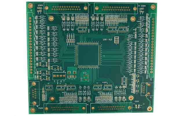
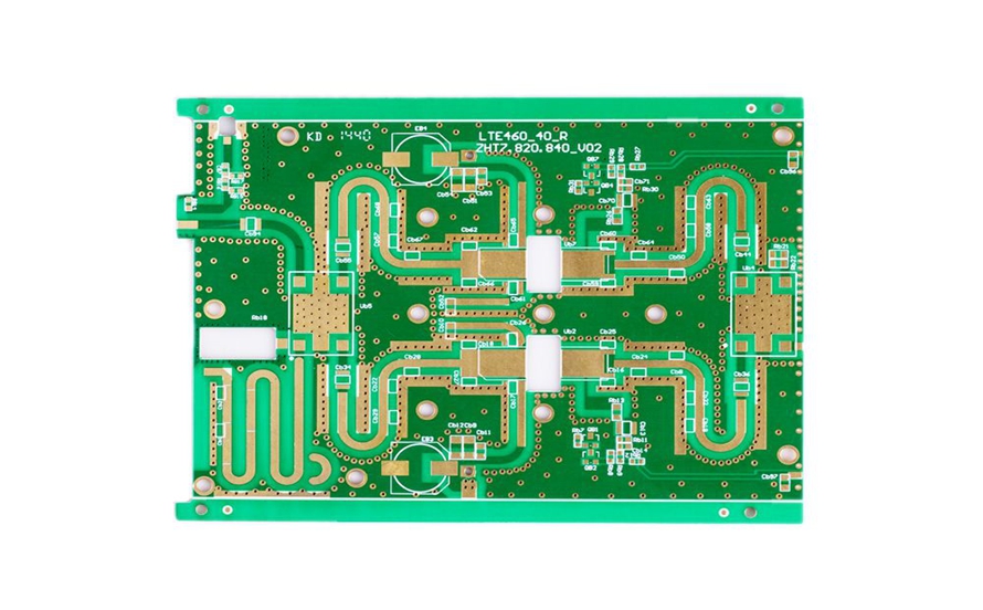
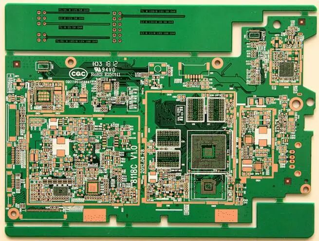
What is an Impedance Controlled PCB? An Impedance Controlled PCB is a printed circuit board designed and manufactured to maintain a specific characteristic impedance for signal traces, ensuring consistent signal transmission. In high-speed and RF designs, the PCB trace behaves like a transmission line. Without proper impedance control, signals can suffer from reflection, distortion, and...
HomeTag
Impedance Controlled PCB - KKPCB
As electronic devices continue to operate at higher speeds, maintaining signal integrity becomes a critical design challenge. Variations in impedance along a signal path can cause reflection, signal loss, and timing issues, potentially compromising system performance. Impedance controlled PCBs are specifically designed to maintain a consistent impedance across high-speed traces, ensuring reliable signal transmission in...
What Is a 5G mmWave PCB? A 5G mmWave PCB is a specialized printed circuit board designed to handle millimeter-wave (mmWave) signals used in 5G wireless communication systems. Operating at extremely high frequencies, typically 24 GHz to 100 GHz, mmWave PCBs require precise impedance control, low dielectric loss, and high signal integrity to ensure efficient...
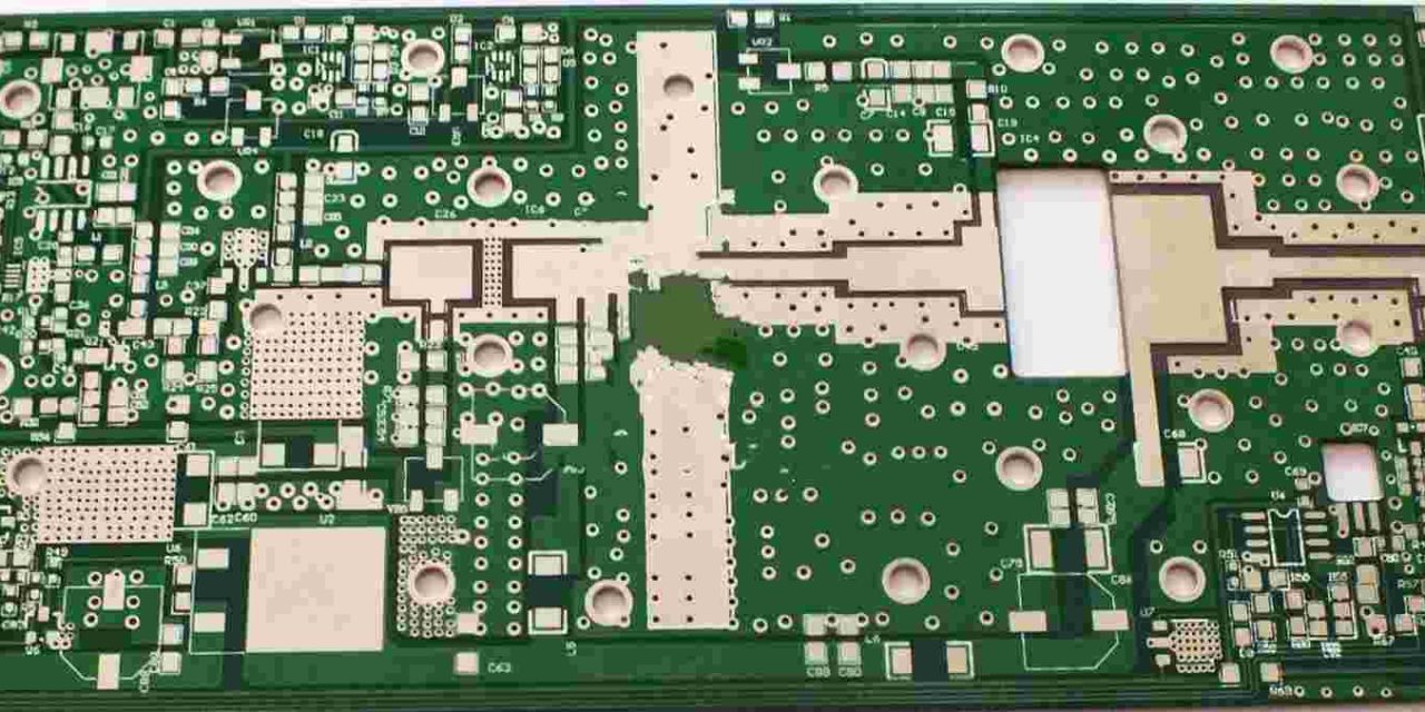
RF PCBs (Radio Frequency Printed Circuit Boards) are widely used in modern high-frequency electronic systems. From wireless communication equipment to radar modules and satellite electronics, RF PCBs play a critical role in ensuring stable signal transmission and minimal signal loss. Unlike standard PCBs, RF PCBs operate in the MHz to GHz frequency range. This means...
What Is an Impedance Controlled PCB? An Impedance Controlled PCB is a printed circuit board designed to maintain precise characteristic impedance along signal traces. This is critical for high speed digital circuits, RF communication, and microwave systems, where mismatched impedance can cause: Signal reflection Crosstalk Data errors Timing skew Impedance control ensures reliable signal integrity...
A controlled impedance PCB prototype is a critical step in validating high-speed and high-frequency electronic designs before mass production. As data rates increase and signal frequencies rise, maintaining precise impedance values becomes essential to ensure signal integrity, reduce reflection, and minimize transmission loss. Controlled impedance PCB prototypes are widely used in applications such as high-speed...
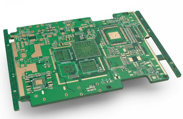
What Is a High Speed PCB? A High Speed PCB is a printed circuit board designed to support high-speed digital signals, typically operating at multi-gigabit data rates. These PCBs are essential for modern electronics where signal integrity, timing accuracy, and low noise are critical. High speed PCBs are widely used in servers, networking equipment, semiconductor...
What Is a Duroid 6010 PCB? A Duroid 6010 PCB is a high-frequency printed circuit board fabricated using Rogers RT/duroid® 6010 laminate. Unlike low-Dk RF materials, Duroid 6010 features a high dielectric constant, enabling compact circuit design and size reduction for microwave and RF systems. Duroid 6010 PCBs are widely used when miniaturization and impedance...
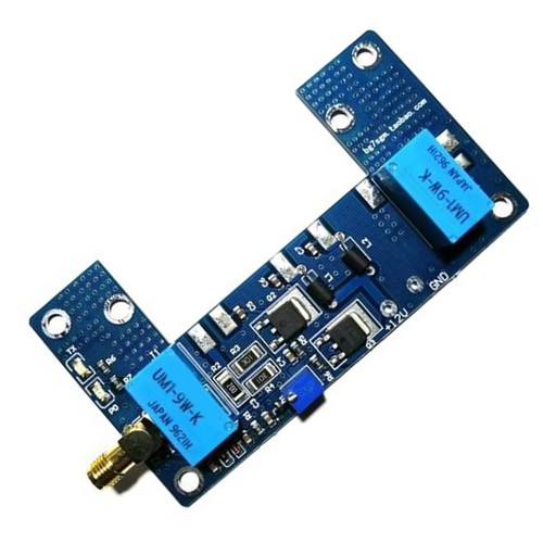
What Is an RF Transceiver PCB? An RF Transceiver PCB is a specialized printed circuit board used in radio frequency transmission and reception systems. It integrates RF transmit (TX) and receive (RX) circuits on the same board, requiring precise control of signal integrity, impedance, and electromagnetic performance. RF transceiver PCBs are critical in modern wireless...
What Is a Low Loss PCB? A Low Loss PCB is a printed circuit board engineered to reduce signal attenuation, insertion loss, and phase distortion during signal transmission. It is essential for high-speed digital, RF, and millimeter-wave applications, where even small signal losses can significantly impact system performance. Low loss PCBs are widely used in...

