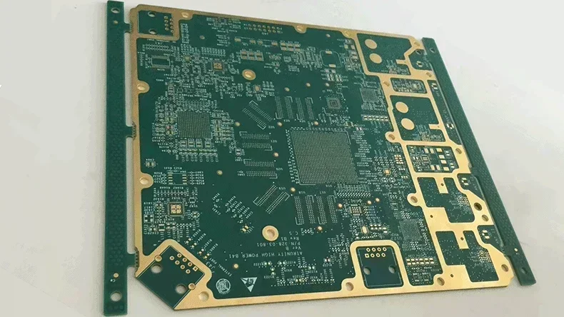
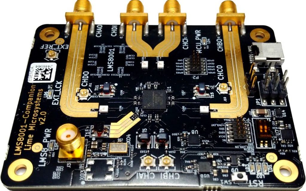
impedance control PCB - KKPCB
 
HomeTag

impedance control PCB - KKPCB

Controlled Impedance PCB Prototype: Reducing Risk in High-Speed and RF Design Validation

For high-speed digital and RF electronic systems, signal integrity is one of the most critical design challenges. A controlled impedance PCB prototype plays a key role in validating design assumptions, manufacturing tolerances, and electrical performance before moving into mass production. Building controlled impedance into the prototype stage significantly reduces technical and production risk. What Is...

Controlled Impedance PCB Prototype: Precision Prototyping for High-Speed and RF Designs

As data rates and operating frequencies continue to increase, signal integrity becomes a critical factor even at the prototype stage. A controlled impedance PCB prototype allows engineers to validate high-speed and RF signal performance before entering volume production. Accurate impedance control during PCB prototyping helps reduce reflections, minimize signal loss, and ensure design reliability from...

Professional High Frequency PCB OEM for RF and High-Speed Communication Systems

With the rapid evolution of RF, microwave, and high-speed communication technologies, PCB performance has become a critical factor in system reliability and signal integrity. Selecting a professional high frequency PCB OEM is essential for manufacturers developing RF and high-speed communication systems that operate in GHz and millimeter-wave environments. A qualified high frequency PCB OEM combines...

Building Reliable High-Speed Electronics with Controlled Impedance PCB Architectures

Introduction: Why Controlled Impedance Defines High-Speed Reliability As high-speed electronics push into multi-gigabit data rates and high-frequency RF domains, signal behavior is no longer dominated by logic thresholds—it is governed by transmission line physics. In these systems, every PCB trace behaves as a controlled impedance structure, and any deviation can introduce reflections, timing skew, and...

Controlled Impedance PCB Engineering for High-Speed Digital and High-Frequency RF Applications

A Controlled Impedance PCB is a critical foundation for modern high-speed digital systems and high-frequency RF applications. As signal rise times shrink and operating frequencies extend into multi-GHz ranges, PCB interconnects must behave as predictable transmission lines rather than simple copper connections. Controlled Impedance PCB design ensures signal integrity, phase stability, and EMI compliance across...

High Speed PCB Engineering for Signal Integrity, Power Integrity, and Ultra-Low-Latency Electronic Systems

As modern electronics become faster, more compact, and more data-intensive, the High Speed PCB has evolved into a critical engineering platform for communication systems, servers, AI accelerators, radar units, embedded computing modules, and advanced industrial electronics. A well-engineered High Speed PCB ensures clean signal transmission, stable power behavior, and low-jitter operation across multi-gigabit channels. High-speed...

Achieve Low-Loss Transmission and Stable Impedance Performance with Double Layer HF PCB Engineering for High-Frequency Communication Systems

A Double Layer HF PCB may appear structurally simple, yet in high-frequency engineering it provides a remarkably efficient platform for low-loss propagation, stable impedance, and predictable electromagnetic behavior. When RF designers need high-frequency stability without the cost or stackup escalation of multilayer PCBs, a Double Layer HF PCB offers the ideal balance between manufacturability and...

Drive Ultra-Stable Dk/Df Performance and High-Power Efficiency Using RO5880 PCB Architectures in Mission-Critical Aerospace and Communication Systems

Mission-critical aerospace and high-frequency communication systems depend on PCB materials that deliver absolute electrical stability, consistent power efficiency and repeatable RF performance under extreme thermal, mechanical and radiation environments. RO5880 PCB architectures have become a foundation for these systems because they offer exceptionally stable Dk/Df, low insertion loss and predictable phase behavior across microwave and...

Advancing Electronic Engineering Through High-Precision PCB Prototype Fabrication Technologies

Modern electronics development depends on fast, accurate, and predictable PCB prototype fabrication. As device complexity rises—spanning RF modules, 5G transceivers, AI accelerators, and densely integrated consumer electronics—engineering teams rely on high-precision prototyping to validate architectures before mass production. PCB prototype technology has evolved from simple single-layer boards into a highly automated, material-specific, impedance-controlled manufacturing discipline....

Boost High-Q Resonance and Ultra-Stable Impedance Control with High-Frequency Sensor PCB Structures for Aerospace Navigation Sensors

Aerospace navigation sensors operate in a realm where the margin for error is essentially zero. Whether guiding autonomous aircraft, stabilizing flight control modules, or supporting satellite-assisted positioning, these sensors rely on high-frequency PCB platforms engineered for absolute electrical stability. Achieving high-Q resonance and ultra-consistent impedance is not just a design preference—it is the foundation of...