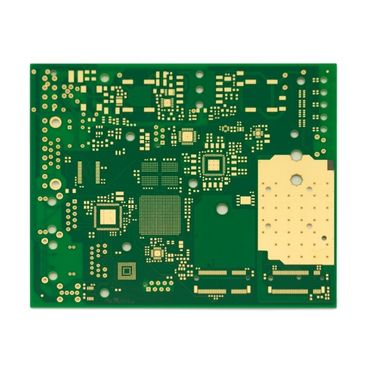
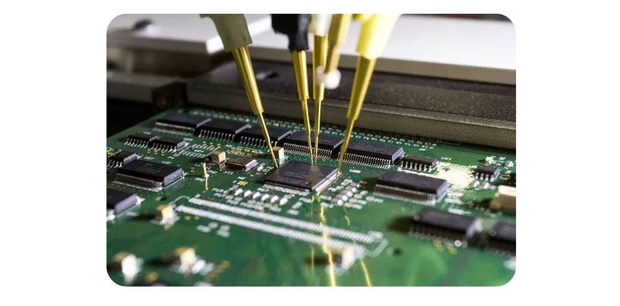
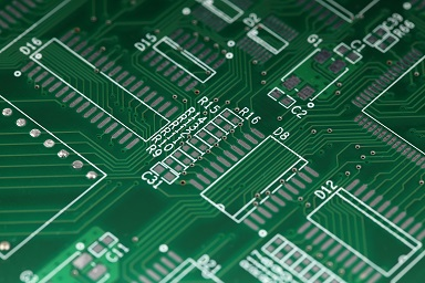
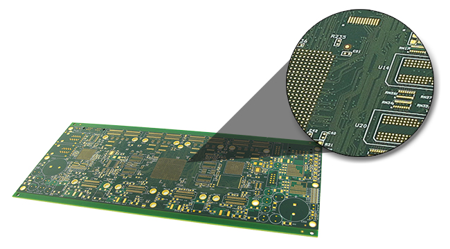
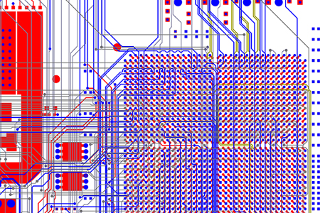
high-speed PCB - KKPCB
 
HomeTag

high-speed PCB - KKPCB

Designing High Layer Count PCBs for Complex Signal, Power, and Thermal Integrity Challenges

As electronic systems continue to integrate higher data rates, greater power density, and tighter form factors, high layer count PCBs have become a foundational platform for modern hardware architecture. Designs exceeding 16, 20, or even 30 layers are now common in data center equipment, telecommunications infrastructure, aerospace electronics, and industrial control systems. However, increasing layer...

Controlled Impedance PCB Engineering for High-Speed Digital and High-Frequency RF Applications

A Controlled Impedance PCB is a critical foundation for modern high-speed digital systems and high-frequency RF applications. As signal rise times shrink and operating frequencies extend into multi-GHz ranges, PCB interconnects must behave as predictable transmission lines rather than simple copper connections. Controlled Impedance PCB design ensures signal integrity, phase stability, and EMI compliance across...

Enable Ultra-High Interconnect Density and Signal Integrity with Advanced High Layer Count PCB Architectures

High Layer Count PCB: The Backbone of Complex Electronic Systems A High Layer Count PCB refers to a multilayer printed circuit board typically featuring 16 layers, 24 layers, 32 layers, or more, designed to support complex signal routing, dense interconnections, and advanced power distribution. As electronic systems continue to integrate higher data rates, tighter form...

Enhance Routing Density and Signal Integrity with Buried Via PCB Architectures for High-Density Electronic Systems

Buried Via PCB: Enabling High-Density Interconnection Beyond Conventional Multilayer Boards A Buried Via PCB is a multilayer printed circuit board in which vias connect only internal layers and do not extend to the outer layers. Unlike through-hole vias, buried vias are completely embedded within the PCB stackup, enabling higher routing density, improved signal integrity, and...

Enable Ultra-Complex Routing and Signal Integrity with High Layer Count PCB Architectures for Advanced Electronic Systems

High Layer Count PCB: The Backbone of Ultra-Complex Electronic Integration A High Layer Count PCB refers to a multilayer printed circuit board typically exceeding 12 layers and extending to 20, 30, or even 60+ layers for advanced electronic systems. High layer count PCB designs are essential for applications requiring dense routing, high-speed signal transmission, controlled...

Optimize High-Frequency Signal Integrity and Power Efficiency with Low Dissipation Factor PCB Materials

Why Low Dissipation Factor PCB Matters in High-Frequency Electronics As electronic systems evolve toward higher frequencies, faster data rates, and tighter power budgets, signal loss within the PCB itself becomes a dominant performance constraint. In RF, microwave, mmWave, high-speed digital, and satellite communication systems, even minor dielectric losses can accumulate across long signal paths, directly...

Improve Thermal Reliability and Signal Integrity with High TG PCB Materials for High-Performance Electronic Systems

Engineering Context: Why High TG PCB Is Critical in Modern Electronics As electronic systems continue to push toward higher power density, faster signal speeds, and harsher operating environments, conventional PCB materials increasingly become a reliability bottleneck. Excessive heat, repeated thermal cycling, and dense component placement place enormous stress on standard laminates, often leading to warpage,...

High-Speed PCB Design & Manufacturing Guide | Signal Integrity, Materials & KKPCB Engineering Capabilities

High-Speed PCB: Engineering Principles, Core Challenges & KKPCB Capabilities High-Speed PCB technology is at the center of every modern data-intensive system—from 5G infrastructure and AI servers to autonomous machines and aerospace communication modules. As signal frequencies climb beyond 3 GHz, 10 GHz, even 28–56 Gbps, traditional PCB design rules become insufficient. High-speed PCB engineering demands...

High Speed PCB Engineering for Signal Integrity, Power Integrity, and Ultra-Low-Latency Electronic Systems

As modern electronics become faster, more compact, and more data-intensive, the High Speed PCB has evolved into a critical engineering platform for communication systems, servers, AI accelerators, radar units, embedded computing modules, and advanced industrial electronics. A well-engineered High Speed PCB ensures clean signal transmission, stable power behavior, and low-jitter operation across multi-gigabit channels. High-speed...

Smart Factory PCB Engineering for Intelligent Automation, Real-Time Control, and Industry 4.0 Connectivity

Industrial Automation PCB engineering sits at the core of modern manufacturing, robotics, and process-control systems. In factory environments filled with electrical noise, high temperatures, continuous vibration, and mission-critical timing demands, the Industrial Automation PCB must deliver unwavering reliability, low signal distortion, and stable power delivery. As factories evolve toward smart, interconnected, high-speed architectures, the expectations...