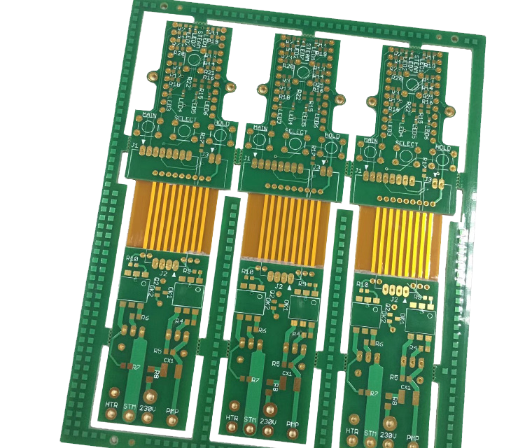
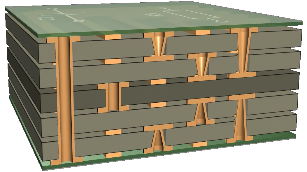
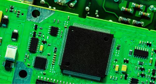
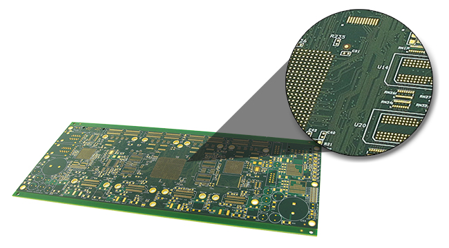
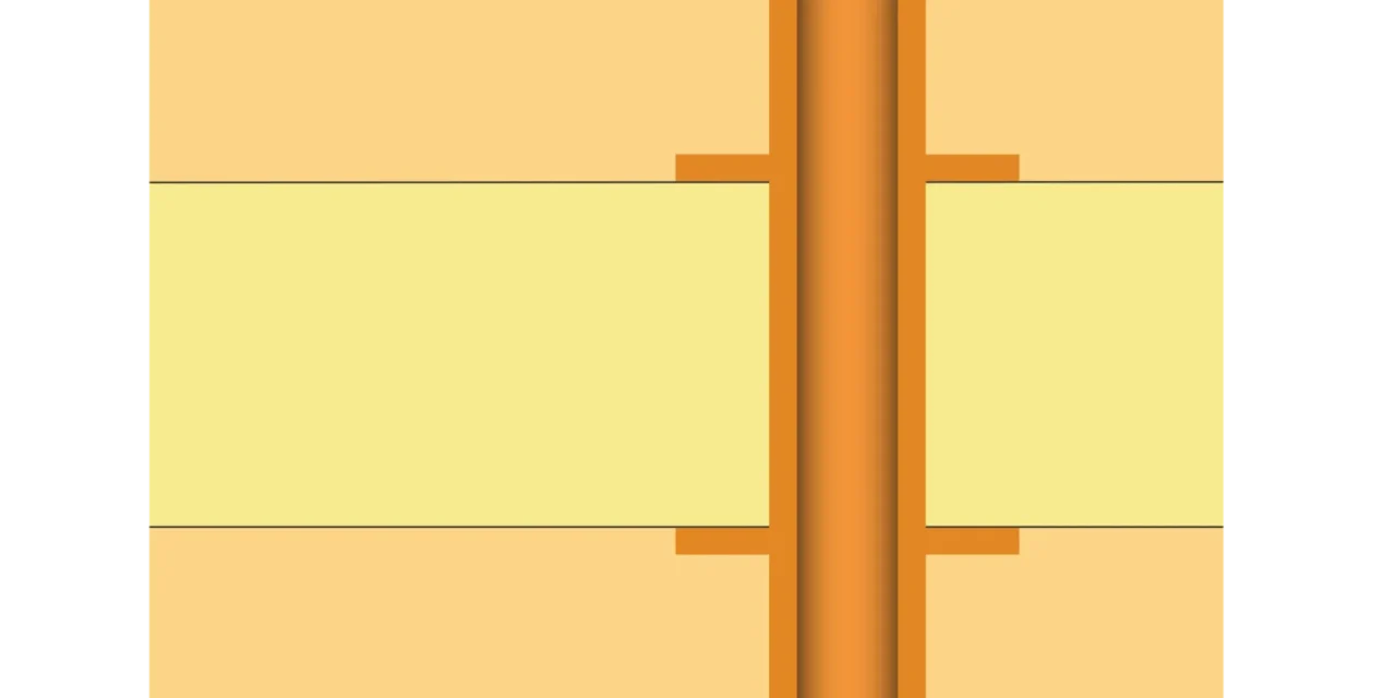
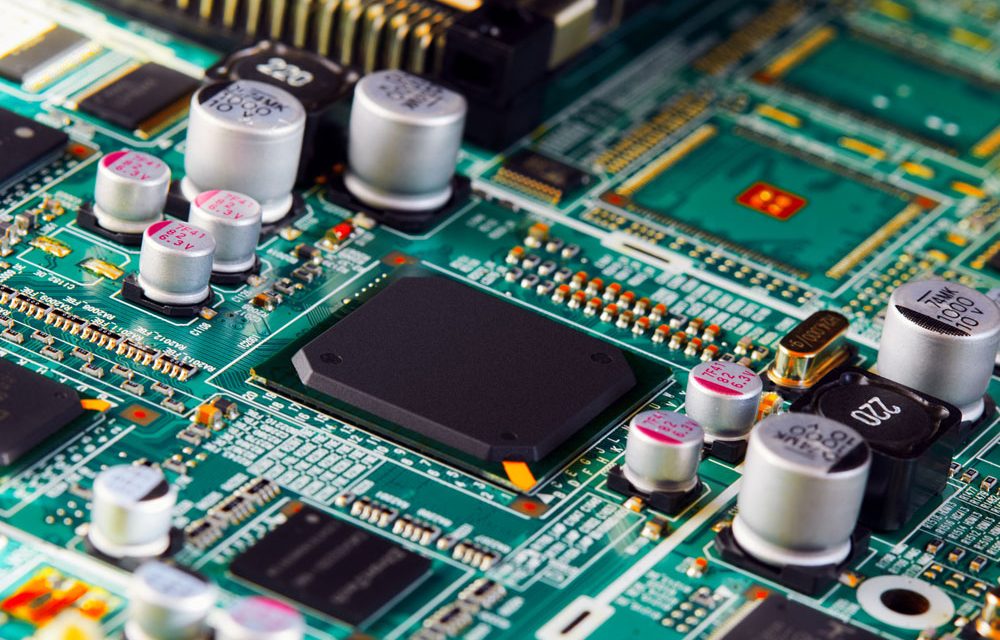
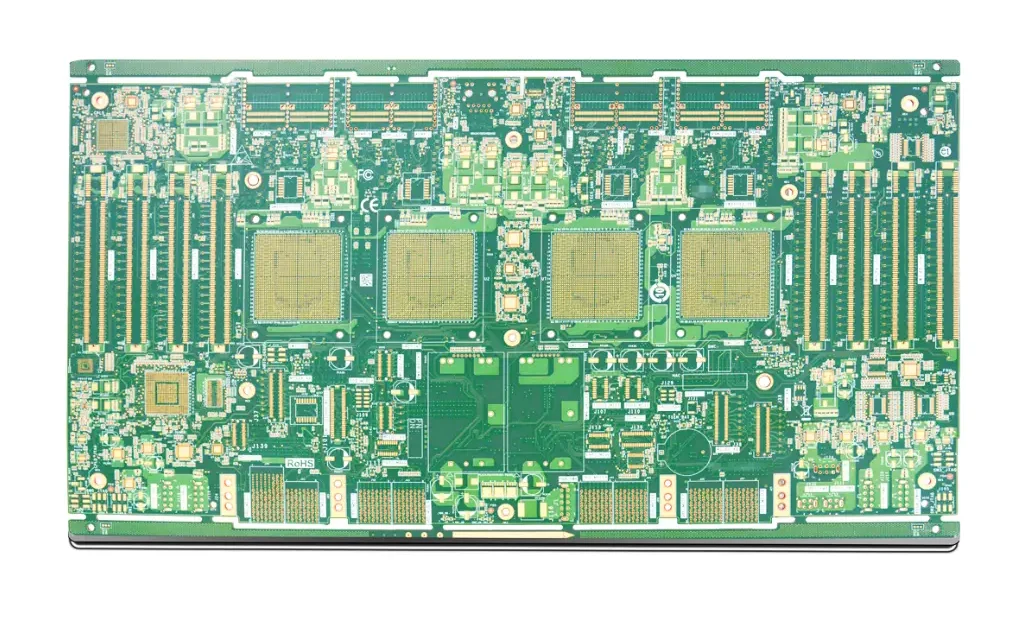
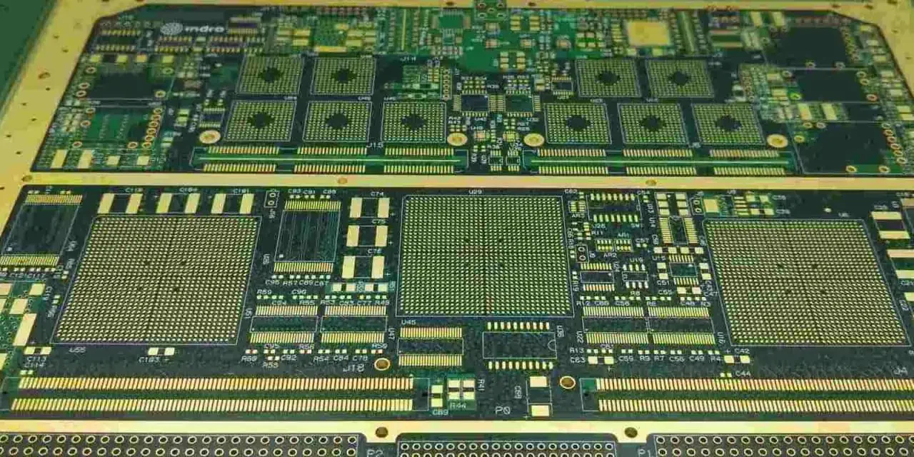
high density pcb - KKPCB
 
HomeTag

high density pcb - KKPCB

High Pin Count IC Test Board for Advanced Semiconductor Testing

What Is a High Pin Count IC Test Board? A High Pin Count IC Test Board is a specialized printed circuit board designed to support integrated circuits with a large number of I/O pins during semiconductor testing. It serves as the electrical interface between the device under test (DUT) and automated test equipment (ATE), enabling...

High Pin Count PCB: Advanced PCB Solutions for High-Density and High-Reliability Applications

A High Pin Count PCB is designed to support electronic components with a large number of I/O pins, such as high-density BGAs, processors, FPGAs, and ASICs. As modern electronic systems demand higher performance, faster data transfer, and increased functionality, high pin count devices have become increasingly common. Manufacturing a reliable high pin count PCB requires...

High Layer Count PCB for Complex and High-Density Electronic Systems

What Is a High Layer Count PCB? A High Layer Count PCB refers to a multilayer printed circuit board containing a large number of copper layers, typically 12 layers and above, designed to support highly complex circuit routing and high-speed signal transmission. High Layer Count PCBs are widely used in advanced electronic systems that require...

Blind Via PCB: High-Density Multilayer PCBs for Advanced Electronics

What Is a Blind Via PCB? A Blind Via PCB is a multilayer PCB that contains vias connecting an outer layer to one or more inner layers without going through the entire board. Unlike through-hole vias, blind vias enable high-density routing and space-saving designs, which are critical for HDI PCBs, high-frequency applications, and compact electronics....

ATE PCB Supplier Solutions: High-Performance Boards for Automated Test Equipment Applications

Automated Test Equipment (ATE) PCBs are critical components in high-precision testing systems for semiconductors, modules, and electronic assemblies. Unlike standard PCBs, ATE PCBs must support high-density routing, controlled impedance, fine-pitch interconnects, and reliable signal integrity, ensuring accurate and repeatable test results. Why ATE PCBs Require Specialized Materials ATE systems often operate under high-speed digital or...

BT Epoxy PCB Design for Dimensional Stability and Electrical Reliability in IC Packaging Applications

A BT Epoxy PCB is a specialized organic substrate widely used in IC packaging, semiconductor interposers, and high-density electronic modules. BT (Bismaleimide Triazine) epoxy resin materials are engineered to provide enhanced thermal stability, low moisture absorption, and excellent dimensional control, making BT Epoxy PCBs a preferred choice for fine-pitch and high-I/O-count packaging environments. Unlike standard...

Fine Line PCB: High Precision PCB Manufacturing for HDI and High-Density Routing

What Is a Fine Line PCB? A Fine Line PCB is a high-precision printed circuit board manufactured with ultra-thin trace width and tight trace spacing, enabling high-density routing for advanced electronic products. Compared with standard PCB technology, Fine Line PCB fabrication focuses on achieving smaller line/space (L/S), higher wiring density, and improved signal performance in...

High Speed Logic PCB: Controlled Impedance and Signal Integrity for Fast Digital Systems

What Is a High Speed Logic PCB? A High Speed Logic PCB is a printed circuit board designed for high-speed digital logic signals that require stable timing, clean waveforms, and reliable data transmission. Unlike standard PCBs, a High Speed Logic PCB must handle fast edge rates, high-frequency harmonics, and strict signal integrity requirements for interfaces...

Signal Integrity PCB: Designing for Clean Signals, Low Noise, and High-Speed Performance

What Is a Signal Integrity PCB? A Signal Integrity PCB is a printed circuit board specifically designed and manufactured to ensure high-speed signals remain stable, clean, and reliable from transmitter to receiver. In modern electronics, as data rates increase and edge rates become faster, signal integrity (SI) becomes one of the most critical performance factors...

Fine Line PCB: Precision Routing for High-Density and High-Speed Electronics

What Is a Fine Line PCB? A Fine Line PCB is a printed circuit board designed with ultra-thin traces and narrow spacing, typically under 4 mils (0.1 mm), enabling high-density interconnections for compact electronic devices. Fine line PCBs are essential in applications where space constraints, high-speed signals, and precise routing are required, such as 5G...