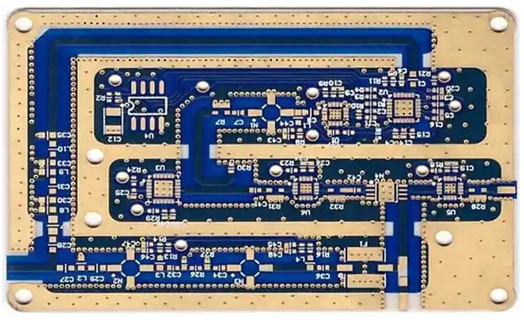
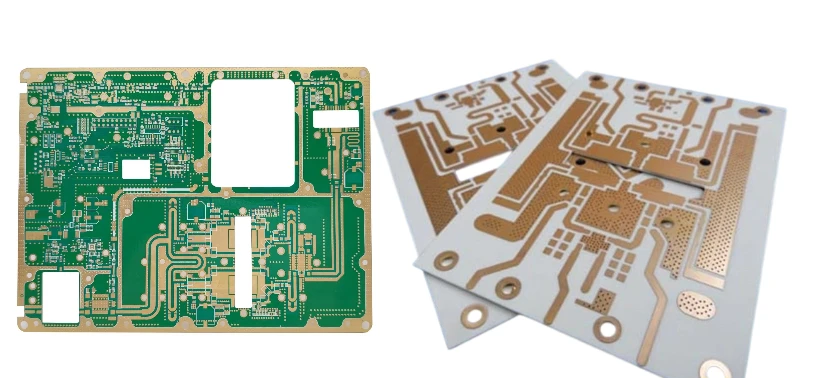
Differential Pair PCB - KKPCB
 
HomeTag

Differential Pair PCB - KKPCB

Signal Integrity PCB: Designing for Clean Signals, Low Noise, and High-Speed Performance

What Is a Signal Integrity PCB? A Signal Integrity PCB is a printed circuit board specifically designed and manufactured to ensure high-speed signals remain stable, clean, and reliable from transmitter to receiver. In modern electronics, as data rates increase and edge rates become faster, signal integrity (SI) becomes one of the most critical performance factors...

High Frequency Signal PCB: Ensuring Optimal Performance for High-Speed Electronics

What Is a High Frequency Signal PCB? A High Frequency Signal PCB is a printed circuit board specifically engineered to handle high-speed and high-frequency signals with minimal signal loss and optimal signal integrity. These PCBs are crucial in RF communication, 5G modules, high-speed computing, IoT devices, and automotive radar systems. High frequency signals require careful...

Differential Pair PCB: Precision Routing for High-Speed Signal Integrity

What Is a Differential Pair PCB? A Differential Pair PCB is a printed circuit board that routes signal pairs with equal and opposite voltages to maintain signal integrity and reduce noise. Differential pairs are essential for high-speed digital interfaces, high-frequency analog signals, and RF communication systems. By using precisely matched trace lengths, controlled spacing, and...

High Speed Logic PCB: Ensuring Signal Integrity and Reliable Digital Performance

What Is a High Speed Logic PCB? A High Speed Logic PCB is a printed circuit board engineered to handle high-frequency digital signals with minimal distortion, noise, or timing errors. These PCBs are critical in applications where fast signal transitions, high data rates, and precise timing are required, such as computer motherboards, networking equipment, 5G...

Signal Integrity PCB Design for High-Speed and High-Frequency Electronics

What Is a Signal Integrity PCB? A Signal Integrity PCB is a printed circuit board specifically designed to preserve the quality, timing, and accuracy of electrical signals as they propagate through high-speed and high-frequency circuits. As signal speeds increase and edge rates become faster, maintaining signal integrity (SI) becomes a critical factor in overall system...

High Speed Logic PCB: Optimized Design for Fast Digital Circuits and Reliable Performance

Introduction to High Speed Logic PCB A High Speed Logic PCB is designed to support ultra-fast digital circuits while maintaining signal integrity, low noise, and reliable operation. These PCBs are critical for modern electronics, where data rates and clock frequencies are continually increasing, such as in computing, networking, 5G communications, automotive ECUs, and IoT devices....

Signal Integrity PCB: Ensuring High-Speed, Low-Noise Performance in Advanced Electronics

What Is a Signal Integrity PCB? A Signal Integrity PCB is engineered to maintain clean, reliable, and distortion-free signal transmission in high-speed and high-frequency electronic systems. Signal degradation, crosstalk, and reflections can compromise system performance, especially in high-speed digital, RF, 5G, IoT, and high-performance computing applications. Signal integrity PCB design ensures consistent impedance, controlled trace...

Differential Pair PCB: High-Speed PCB Design for Signal Integrity and Noise Reduction

What Is a Differential Pair PCB? A Differential Pair PCB is a specialized printed circuit board designed with paired traces carrying equal and opposite signals. This design minimizes electromagnetic interference (EMI), reduces signal crosstalk, and maintains high-speed signal integrity. Differential pair PCBs are critical in applications where accurate high-speed data transmission is required, such as...

High Speed Test PCB: Signal Integrity and Timing Accuracy for High-Speed Digital Validation

As data rates continue to increase, validating high-speed digital interfaces requires test platforms that introduce minimal distortion. The High Speed Test PCB is engineered to act as a transparent signal medium, enabling accurate characterization of high-speed devices and systems. A well-designed high speed test PCB ensures that test results reflect real device performance rather than...

Controlled Impedance PCB Prototype: Accurate Signal Integrity Validation from Design to Production

As data rates and operating frequencies continue to increase, maintaining signal integrity becomes a critical design challenge. A controlled impedance PCB prototype allows engineers to verify impedance accuracy, minimize signal reflection, and validate high-speed or RF performance before entering mass production. By prototyping controlled impedance PCBs early, design risks are reduced and product reliability is...