Controlled Impedance PCB - KKPCB
 
HomeTag

Controlled Impedance PCB - KKPCB

PTFE PCB – Ultra Low Loss High Frequency PCB for RF and Microwave Applications

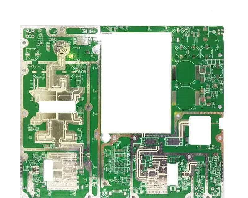
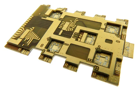
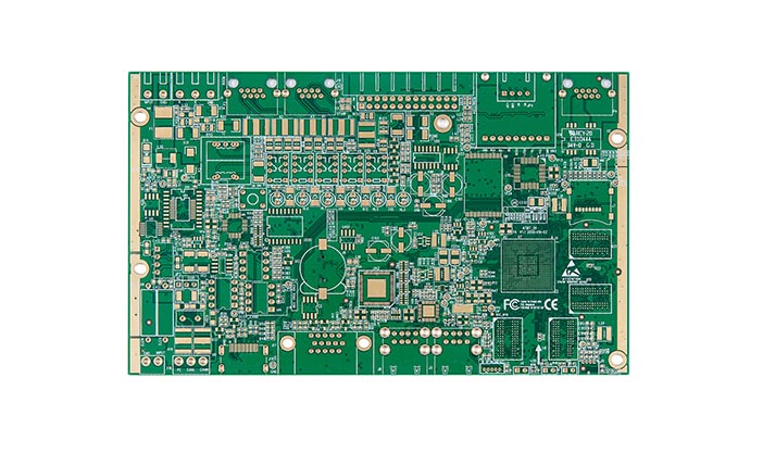
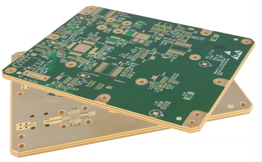
What Is a PTFE PCB? A PTFE PCB is a printed circuit board manufactured using polytetrafluoroethylene (PTFE)-based laminate materials. PTFE is widely recognized for its extremely low dielectric loss, stable electrical properties, and excellent performance at microwave and millimeter-wave frequencies. Because of its superior electrical characteristics, PTFE PCB is commonly used in high-frequency RF systems,...

Rogers PCB – High Performance PCB Solutions for RF and Microwave Applications

What Is a Rogers PCB? A Rogers PCB refers to a printed circuit board manufactured using high-frequency laminate materials developed by Rogers Corporation. These materials are specifically engineered to provide low dielectric loss, stable electrical performance, and reliable operation at high frequencies. Unlike standard FR4 substrates, Rogers materials are designed for RF and microwave applications...

RF Trace PCB – Precision RF Transmission Line Engineering for High Frequency Applications

RF Trace PCB in High Frequency System RF Trace PCB, RF PCB, High Frequency PCB, Microwave PCB, Controlled Impedance PCB, Microstrip PCB, Stripline PCB, CPWG PCB, 5G PCB, Radar PCB, Antenna PCB, Low Loss PCB An RF Trace PCB is a printed circuit board specifically engineered to support stable radio frequency (RF) signal transmission. Unlike...

High Density PCB Design – Engineering Solutions for Complex and Compact Electronic Systems

Engineering Challenges Behind High Density PCB As electronic systems become more compact and functionally integrated, PCB designers are facing increasing layout complexity. A High Density PCB is not simply about placing more components on a board — it requires precise coordination between electrical design, stack-up engineering, manufacturability, and long-term reliability. High density PCB development focuses...

HDI PCB – High Density Interconnect PCB for Advanced Electronic Applications

What Is an HDI PCB? An HDI PCB (High Density Interconnect PCB) is a printed circuit board designed with higher wiring density per unit area compared to traditional PCBs. It typically incorporates microvias, blind and buried vias, fine trace widths, and advanced multilayer stack-ups to support compact and high-performance electronic designs. HDI technology enables smaller...

Load Board PCB – High Precision Interface Board for Semiconductor Testing

What Is a Load Board PCB? A Load Board PCB is a critical interface board used in Automated Test Equipment (ATE) systems for semiconductor device testing. It connects the tester to the device under test (DUT), transmitting signals, power, and measurement data with high accuracy and stability. Load boards are specifically engineered to support high...

ATE Test PCB – High Precision PCB for Automated Test Equipment Applications

ATE Test PCB for Semiconductor and IC Testing An ATE Test PCB (Automated Test Equipment PCB) is a high-precision printed circuit board designed for semiconductor and integrated circuit testing systems. It serves as the electrical interface between the test system and the device under test (DUT), ensuring accurate signal transmission, stable power delivery, and reliable...

Buried Via PCB – High Density Multilayer PCB with Internal Via Interconnection

What Is a Buried Via PCB? A Buried Via PCB is a multilayer printed circuit board that uses vias connecting only internal layers, without extending to the outer surface layers. Unlike through-hole vias that pass through the entire board thickness, buried vias are fully embedded within the PCB stack-up. This structure improves routing density, reduces...

Rigid-Flex PCB – Flexible and Rigid Hybrid PCB for Compact and High Reliability Applications

What Is a Rigid-Flex PCB? A Rigid-Flex PCB combines rigid circuit board sections with integrated flexible circuit layers into a single unified structure. This hybrid design allows the board to bend in specific areas while maintaining structural stability in others. Unlike traditional assemblies that connect separate rigid boards using cables or connectors, rigid-flex technology integrates...

Double Layer HF PCB – High Frequency Two Layer PCB for RF and Microwave Applications

Double Layer HF PCB for RF and Microwave Systems A Double Layer HF PCB (High Frequency PCB) is a two-layer printed circuit board designed specifically for RF and microwave signal transmission. Unlike standard double-sided FR4 boards, HF PCBs use low-loss, stable dielectric materials to ensure reliable signal performance at high frequencies. Double layer high frequency...