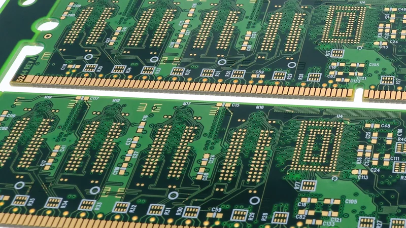
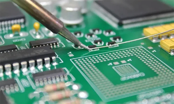
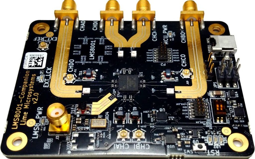
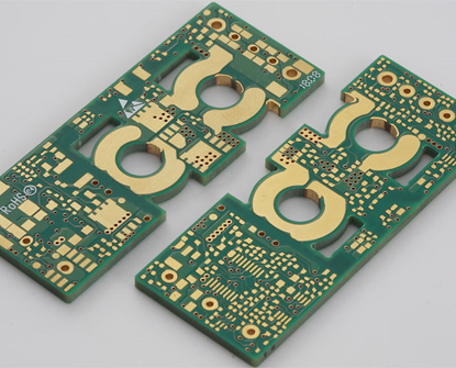
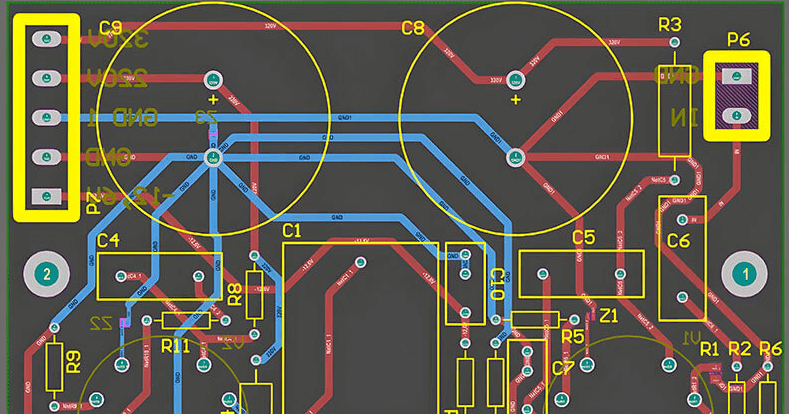
Advanced Engineering Technologies for PCB & PCBA Solutions - KKPCB
 
HomeCategory

Advanced Engineering Technologies for PCB & PCBA Solutions - KKPCB

Electromagnetic Compatibility (EMC) Challenges in PCB Design

With rising PCB trace speeds, electromagnetic compatibility (EMC) becomes increasingly crucial in PCB design. Key EMC attributes are essential to analyze in order to identify and mitigate potential interference sources. Below are the five critical attributes to consider during EMC analysis, followed by practical layout strategies. 1. Key Component Size and Trace Length Radiating Device Size: The...

PCB Design Wiring Rules: Best Practices for Optimal Performance

Wiring in PCB design is a critical step that directly impacts product performance. With the complexities of single-sided, double-sided, and multi-layer wiring, and methods like automatic and interactive wiring, designers must carefully consider routing techniques. Below, we outline essential PCB wiring rules and guidelines for achieving effective signal integrity, power management, and ground control. 1. Key Wiring Rules...

Essential Checkpoints for Final Stages of PCB Design

Inexperienced PCB designers often overlook critical checks in the later design stages, leading to issues like inadequate line width, misplaced silkscreens, and insufficient spacing near sockets. These errors can cause electrical or manufacturing issues, potentially requiring redesigns and increasing production costs. Below is a comprehensive list of essential PCB design checkpoints to ensure product quality and manufacturability....

How to Reduce Circuit Board Noise

In PCB design, a well-designed circuit can still produce noise during testing, leading to performance issues or even requiring a board redesign. Below, we explore strategies to reduce circuit board noise effectively. Functional Module Separation A high-performance board will often have a clear layout of functional modules. A functional module is a collection of circuits and components dedicated...

Precautions for PCB Design

In PCB design, circuit layout is fundamental for engineers. However, even experienced engineers may overlook critical details in basic PCB design, which can lead to errors. Sometimes, these errors may cause problems or even a complete failure of the circuit when converted into a PCB. To help engineers avoid redesigns and improve work efficiency, here are...

Grounding Methods for Multi-Layer PCB Boards

Grounding Method for Multi-Layer PCB Boards (I) Four-layer PCBs are typically used for high-density, high-frequency applications and offer more than 20 dB better electromagnetic compatibility (EMC) compared to two-layer boards. In a four-layer board setup, a complete ground plane and a full power plane can be used. This allows the various circuit ground wires to be connected...

Practical Experience in PCB ESD Design

Recently, I have been conducting ESD (Electro-Static Discharge) testing on various electronic products. From the test results, I realized that ESD is crucial: if the PCB design lacks proper ESD protection, static electricity can cause devices to freeze or even damage their components. Previously, I only understood that ESD could damage individual components, but now I see...

Overview of DFM Technical Requirements for PCB Process

Design for Manufacturability (DFM) optimizes designs for the manufacturing process, making it an essential component of concurrent engineering. By considering factors such as manufacturability and assembly requirements early in the design phase, DFM streamlines production, bridges CAD-CAM communication, and enhances product reliability. Here, we cover general technical requirements for DFM in PCB manufacturing. I. General Requirements...

Common Standards in Printed Circuit Boards (PCB)

PCB manufacturing relies on standardized guidelines to ensure consistent quality and reliability across various applications. The following list covers the most widely recognized standards from the IPC, EIA, and JEDEC organizations, essential for quality assurance in PCB design, assembly, and testing. Key PCB Standards and Guidelines ESD Control IPC-ESD-2020: This standard sets requirements for electrostatic discharge (ESD)...

Guide to Restoring Circuit Diagrams from Physical PCBs

Often, products come without a circuit schematic, making it challenging to understand the PCB’s functionality and design principles. When faced with such a situation, follow these steps to reverse-engineer and restore the circuit diagram. This guide provides detailed instructions for accurately translating a physical PCB back into a schematic diagram. Steps to Restore a Circuit...