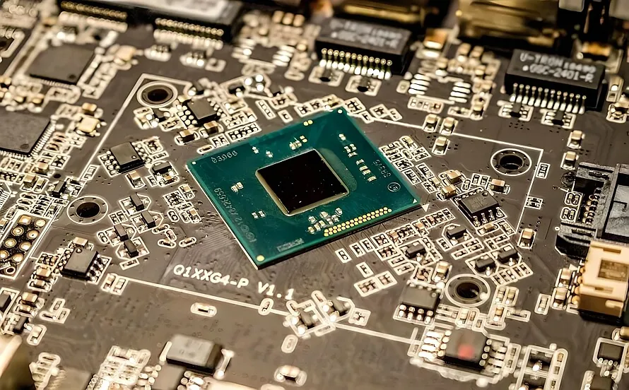
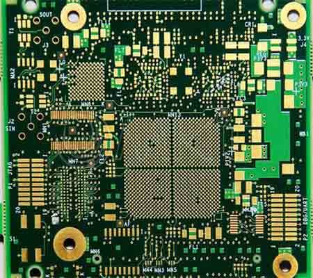
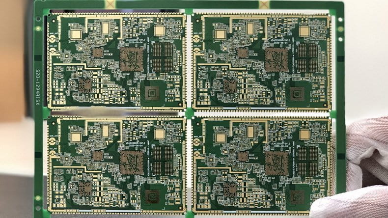
High Speed PCB for Modern Digital Systems As data rates continue to increase in communication, computing, and semiconductor applications, PCB design must evolve to maintain signal integrity and stable performance. A High Speed PCB is specifically engineered to support high-frequency digital signals, fast edge rates, and high bandwidth transmission. Unlike standard PCBs, high speed boards...
HomeCategory
Advanced Engineering Technologies for PCB & PCBA Solutions - KKPCB
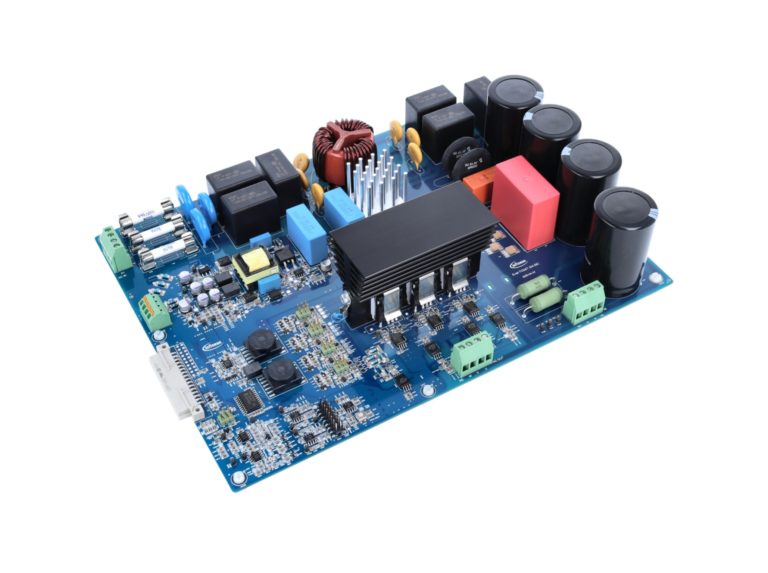
SiC PCB: Supporting the Next Generation of Power Electronics With the rapid growth of electric vehicles, renewable energy systems, and industrial power modules, Silicon Carbide (SiC) devices are becoming a key technology in modern power electronics. Compared to traditional silicon components, SiC devices operate at higher voltages, higher temperatures, and higher switching frequencies. However, these...
Robotics PCB: Powering Intelligent Automation with Precision and Reliability As robotics technology rapidly advances across industrial, medical, logistics, and consumer sectors, the demand for highly reliable and performance-driven printed circuit boards continues to grow. A Robotics PCB serves as the control backbone of robotic systems, enabling motion control, sensor integration, communication, and power management within...
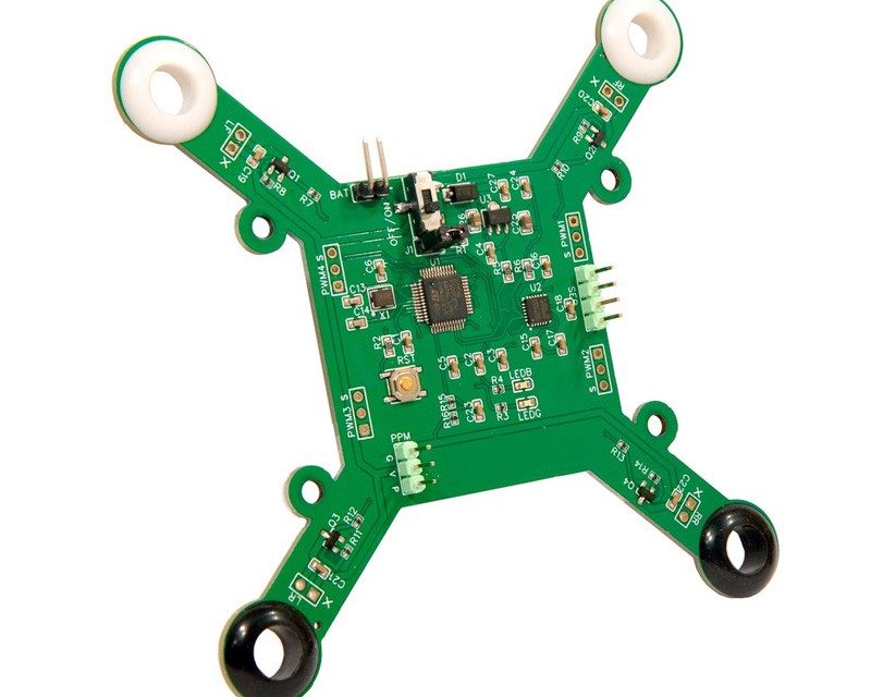
UAV PCB for Advanced Drone and Aerial Systems A UAV PCB (Unmanned Aerial Vehicle PCB) is a high-performance printed circuit board used in drone systems to support flight control, real-time communication, navigation, and power distribution. UAV platforms demand compact size, lightweight construction, stable signal integrity, and resistance to vibration and temperature variation. As drone technology...
ADAS PCB for Automotive Safety and Intelligence ADAS PCB (Advanced Driver Assistance Systems PCB) is a high-reliability printed circuit board used in modern automotive electronic systems that enhance vehicle safety, automation, and driving intelligence. ADAS systems integrate multiple high-speed sensors and processing modules, including: Radar modules (24GHz / 77GHz) Camera control boards LiDAR systems Ultrasonic...
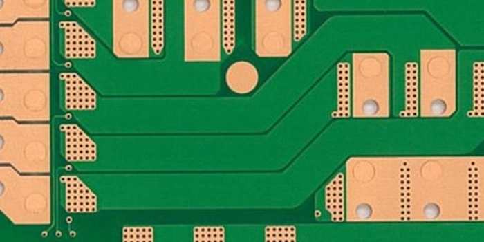
High Current PCB for Demanding Power Applications As power electronics continue to evolve, many modern systems require printed circuit boards capable of handling significantly higher current levels without overheating or performance degradation. A High Current PCB is specifically engineered to carry elevated current loads through optimized copper thickness, reinforced trace design, and enhanced thermal management...
Microvia PCB for High Density Interconnect (HDI) Design As electronic products continue to shrink in size while increasing in functionality, traditional through-hole PCB structures are no longer sufficient. Microvia PCB technology enables higher routing density, improved signal integrity, and compact multilayer stackups, making it essential for modern high-performance electronics. Microvias are laser-drilled vias typically with...
What Is a Multilayer PCB? A Multilayer PCB is a printed circuit board composed of three or more conductive copper layers laminated together with insulating dielectric materials. Compared to single-sided or double-sided boards, Multilayer PCB technology allows significantly higher circuit density and more complex routing structures. Modern electronic systems increasingly require compact size, high speed...
What Is Fine Pitch PCB? A Fine Pitch PCB refers to a printed circuit board designed with extremely small trace width and spacing to support high pin count and fine pitch components. It is commonly used in advanced electronic systems where compact design, high integration, and precise routing are essential. Fine pitch designs are typically...
What Is an IoT IC Test PCB? An IoT IC Test PCB is a specialized printed circuit board used for validating and testing integrated circuits (ICs) designed for Internet of Things (IoT) applications. These PCBs are commonly used in semiconductor test environments such as: Automated Test Equipment (ATE) systems Load boards Probe card assemblies Burn-in...

