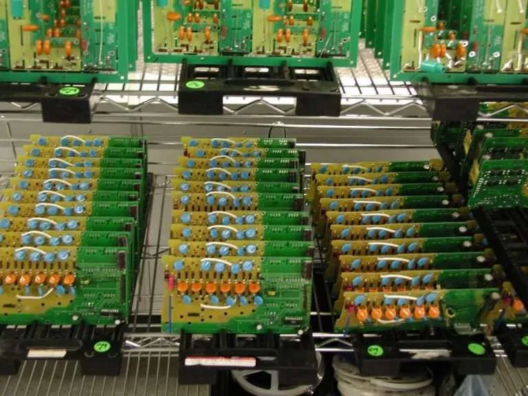
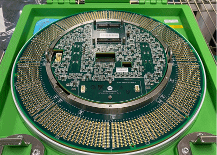
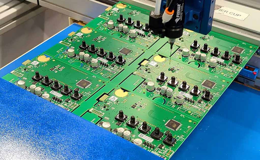
Advanced Engineering Technologies for PCB & PCBA Solutions - KKPCB
 
HomeCategory

Advanced Engineering Technologies for PCB & PCBA Solutions - KKPCB

Detailed Explanation of PCB Manufacturing Process and Precautions

High-quality PCB production begins with high-quality design. Huaqiang PCB manufacturing heavily relies on the cooperation of the design process. Engineers, please design your PCBs according to the detailed explanation of the conventional production process below. Design Parameters for PCB Manufacturing 1. Via (Conductive Hole) Minimum hole diameter: 0.3mm (12mil) The minimum via hole diameter is 0.3mm, and...

Mobile Phone PCB Layout: Key Considerations and Wiring Best Practices

PCB layout in mobile phone design requires meticulous attention to minimize risks and ensure optimal performance. With multiple layers dedicated to various functions, specific guidelines help maintain signal integrity and reduce electromagnetic interference (EMI). Below are the detailed issues and wiring principles to consider in mobile phone PCB layout, especially for complex components like RF circuits...

How to Deal with Power Supply Noise Interference in PCB Design

Power supply noise interference is a critical challenge in PCB design, particularly in high-frequency circuits. Noise from the power supply can significantly impact signal integrity and overall circuit performance. This article provides an in-depth analysis of power supply noise, its causes, and practical strategies to mitigate interference in PCB design. Understanding Power Supply Noise Power supply...

Basic Rules for PCB Layout and Wiring

I. Component Layout Rules Module-Based Layout: Group related components that serve the same function into a module. Separate digital and analog circuits to minimize interference. Clearance Around Holes: Non-mounting holes (e.g., positioning holes): Keep a 1.27mm clearance around them. Mounting holes (e.g., screw holes): Maintain 3.5mm clearance for M2.5 screws and 4mm for M3 screws. Avoid Vias Under Components: Do not place vias under horizontal...

PCB Material Selection Guide

PCB is the most important part of electronics. Alternately, the acronym has also accounted for printed wiring boards and printed wiring cards, which are essentially the same thing. Due to the crucial role of these boards in everything from computers to calculators, PC board material selection should be undertaken with care and knowledge for electrical...

How Are Printed Circuit Boards Manufactured?

Circuit boards play a key role in making sure electronic products work properly. They provide structural support and link all the electrical parts together. Whether it’s in smartphones, laptops, or household devices, none could operate without a PCB. This guide will introduce you to the components of a printed circuit board and help you understand the manufacturing process....

PCB Plating Hole Filling Technology

The output value of the global electroplating PCB industry accounts for the rapid growth of the proportion of the total output value of the electronic component industry. It is the industry with the largest proportion in the electronic component industry. It occupies a unique position. The volume of electronic products is becoming lighter and thinner. Design method...

Why EMC Compliance important in Motor Control PCB Design

Ensuring Electromagnetic Compatibility (EMC) compliance in motor control PCBs is essential to avoid interference issues, maintain system reliability, and ensure regulatory approval for market access. Here’s a breakdown of why EMC compliance matters and how to achieve it. 1. Why is EMC Compliance Important? Ensures Reliable Operation Without proper EMC measures, Electromagnetic Interference (EMI) can disrupt nearby electronic devices, causing system...