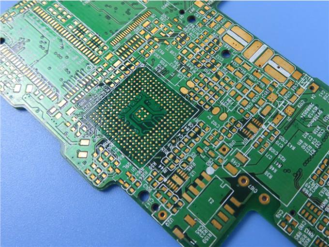
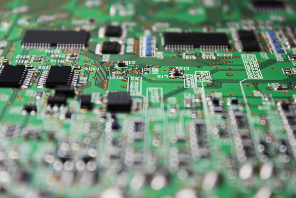
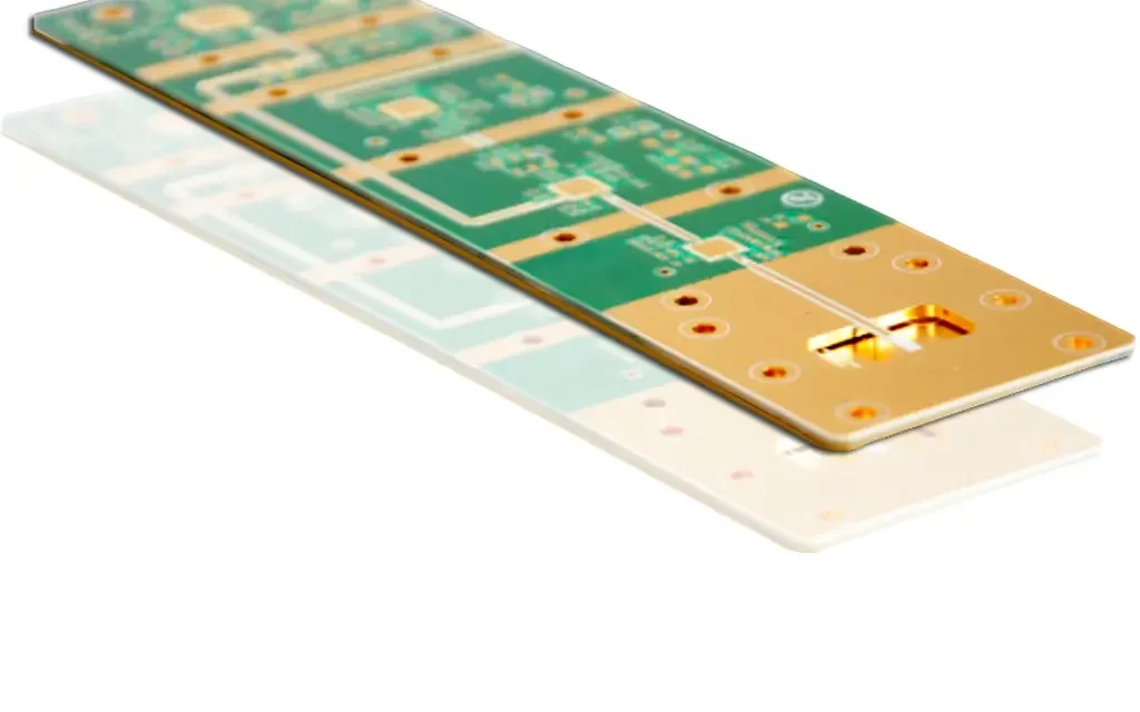
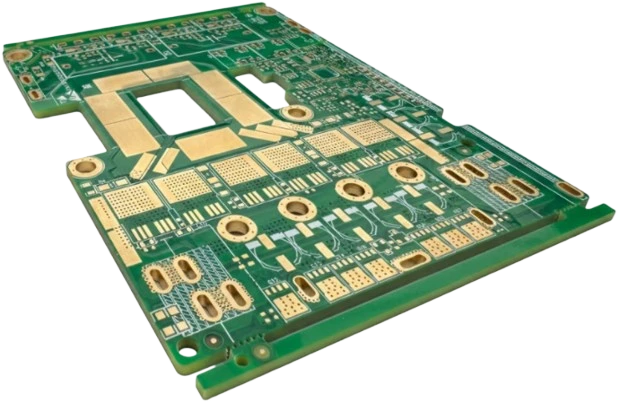
Advanced Engineering Technologies for PCB & PCBA Solutions - KKPCB
 
HomeCategory

Advanced Engineering Technologies for PCB & PCBA Solutions - KKPCB

High-Speed PCB Design Guide 7: Reducing RF Effects in PCB Interconnection Design

PCB interconnections can be categorized into three main types: chip-to-PCB, interconnections within the PCB, and PCB-to-external devices. High-frequency PCB designs require addressing RF effects at these interconnection points to ensure optimal performance. This guide covers techniques for minimizing RF interference, crosstalk, and return loss across these interconnection types. The Impact of High-Frequency Signals on PCB Design As...

High-speed PCB design guide 6: Application technology of PowerPCB in PCB design

PCBs are critical in electronic devices, ensuring electrical connections between components. With increasing circuit density, proper PCB design techniques are essential to ensure reliability and reduce interference. General PCB Design Principles Wiring Guidelines: Avoid Parallel Wires: Insert ground wires between input/output wires to reduce feedback. Conductor Width: Choose widths based on current requirements (e.g., 1.5mm width for 2A current). Conductor Bends: Use...

High-Speed PCB Design Guide 5: Noise Reduction Technology for DSP Systems

With the rise of high-speed DSPs (Digital Signal Processors) and peripherals, managing Electromagnetic Interference (EMI) has become a crucial aspect of design. In the past, issues of emission and interference were broadly referred to as EMI or RFI (Radio Frequency Interference). Today, these are part of a more nuanced area: Electromagnetic Compatibility (EMC), which encompasses both emission control...

High-Speed PCB Design Guide 3: Signal Isolation Technology

Signal isolation is critical for transmitting digital or analog signals without direct current flow between the transmitter and receiver. This technology prevents ground loops, mitigates noise, and ensures operator safety in systems with varying ground potentials. Here’s a detailed breakdown of signal isolation technologies, their applications, and design considerations. 1. Signal Isolation Basics Purpose of...

High-Speed PCB Design Guide 2: Avoiding Pitfalls in Mixed-Signal Systems

Designing mixed-signal systems requires attention to placement, trace layout, and protection elements. Today’s SOCs necessitate expertise in digital, analog, and thermal design, pushing system designers to mitigate common pitfalls such as noise, ground bounce, and latch-up. 1. Challenges in Mixed-Signal Systems High-Speed Trends The drive for higher performance in systems like PCs and servers has...

High-Speed PCB Design Guide (Part 1): Basic Concepts of PCB

When designing high-speed PCBs, understanding the core concepts is crucial for ensuring efficiency and functionality. This guide introduces key elements such as layers, vias, pads, and more to help beginners and professionals alike. 1. The Concept of “Layer” PCB layers represent the actual copper foil layers within the board material, unlike virtual layers in software. Modern...

The Significance of Impedance in PCB Design and Manufacturing

Impedance plays a critical role in the functionality, reliability, and performance of printed circuit boards (PCBs). Understanding and managing impedance is essential for ensuring proper signal transmission and maintaining the integrity of the electronic devices that rely on these boards. Below is a detailed analysis of impedance and its importance in PCB design and manufacturing. 1. What...

Comprehensive Guide: From PCB to MCU — Effective Anti-Interference Design

Printed Circuit Boards (PCBs) play a crucial role in supporting and connecting electronic components, while interference can significantly impact their performance. This guide explores anti-interference design principles for PCBs and microcontrollers (MCUs) to ensure reliable operation in high-noise environments. Key Principles of PCB Anti-Interference Design 1. Ground Wire Layout Separate Digital and Analog Ground: Isolate digital and...

Pros and Cons of Copper Coating in PCB Design

Copper coating, also known as copper filling, is an essential aspect of PCB design that plays a key role in reducing impedance, improving anti-interference capabilities, and enhancing the overall efficiency of power delivery. However, there are several factors to consider when applying copper coating, and the effectiveness depends on how well it is executed. Let’s explore the...

Detailed Explanation of PCB Manufacturing Process and Precautions

High-quality PCB production begins with high-quality design. Huaqiang PCB manufacturing heavily relies on the cooperation of the design process. Engineers, please design your PCBs according to the detailed explanation of the conventional production process below. Design Parameters for PCB Manufacturing 1. Via (Conductive Hole) Minimum hole diameter: 0.3mm (12mil) The minimum via hole diameter is 0.3mm, and...