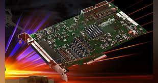
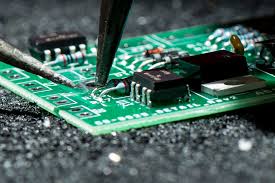
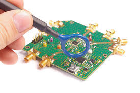
KKPCB Blog – PCB & PCBA Insights, News, and Tips - KKPCB
 

Blog

Explore the KKPCB Blog for the latest PCB manufacturing and assembly news, industry insights, expert tips, and technology trends, helping you stay informed and optimize your electronics projects.
How to optimize PCB design to maximize the performance of superjunction MOSFETs

Based on recent trends, improving efficiency is a key goal, and the trade-off of using slow switching devices for better EMI is not worth it. Superjunctions can improve efficiency in applications where planar MOSFETs struggle. Superjunction MOSFETs significantly reduce on-resistance and parasitic capacitance compared to traditional planar MOSFET technology. The significant reduction in on-resistance and...

Balanced PCB Stack-Up Design Method

In PCB design, one common question arises: if an extra layer is not required for routing, why use it? Reducing the number of layers theoretically makes the board thinner and lowers costs. However, in some cases, adding an additional layer can actually reduce costs. Core Structures of Multilayer PCBs PCBs have two main structures: core structure and...

In the ever-evolving landscape of electronics, high-frequency printed circuit boards (PCBs) are crucial for enabling advanced communication technologies. Among the materials dominating this sector, Rogers 6010 and aluminum-based substrates stand out for their unique properties and performance capabilities. This article explores the characteristics, advantages, and applications of these materials, shedding light on their significance in modern electronics....

IC Replacement Skills in PCB Circuit Design

When replacing an IC in PCB circuit design, the following tips can help designers make more efficient and effective PCB designs. 1. Direct Replacement Direct replacement involves swapping the original IC with a new one without modifying the design. The replacement IC should match the original IC’s main functions, performance indicators, package form, pin configuration, pin...

How to Overcome Challenges in PCB Copy Board Design in the Intelligent Era

With the advancement of policies by the National People’s Congress and the Chinese People’s Political Consultative Conference supporting entrepreneurship and innovation, the electronics industry has been rapidly transforming, propelling us into the intelligent era. In this context, upgrading PCB copy board design technology has become essential. With the expansion of the smartphone and tablet markets,...

Enhancing Anti-Static ESD Function in PCB Design

In PCB design, effective ESD (Electrostatic Discharge) protection can be achieved through strategic layering, layout, and installation adjustments. ESD protection aims to shield delicate semiconductor chips from static electricity originating from humans, the environment, or even other electronic components, which can damage insulation layers, MOSFET and CMOS gates, PN junctions, and wiring. Here are some recommended techniques...

PCB Design Principles for Single-Chip Microcontroller Control Boards

Effective PCB design for single-chip microcontroller (MCU) control boards involves structured layout and routing principles to minimize interference and enhance performance. Proper planning of input/output paths, decoupling, grounding, and component placement is crucial. 1. Component Layout for Reduced Interference Proximity Placement: Place related components, especially noise-sensitive ones (e.g., clock inputs, crystal oscillators, CPU), as close together as possible....

Electromagnetic Compatibility (EMC) Challenges in PCB Design

With rising PCB trace speeds, electromagnetic compatibility (EMC) becomes increasingly crucial in PCB design. Key EMC attributes are essential to analyze in order to identify and mitigate potential interference sources. Below are the five critical attributes to consider during EMC analysis, followed by practical layout strategies. 1. Key Component Size and Trace Length Radiating Device Size: The...

PCB Design Wiring Rules: Best Practices for Optimal Performance

Wiring in PCB design is a critical step that directly impacts product performance. With the complexities of single-sided, double-sided, and multi-layer wiring, and methods like automatic and interactive wiring, designers must carefully consider routing techniques. Below, we outline essential PCB wiring rules and guidelines for achieving effective signal integrity, power management, and ground control. 1. Key Wiring Rules...