kkpcba-Cindy - KKPCB - Page 56 of 75
 
HomeAuthor

kkpcba-Cindy - KKPCB - Page 56 of 75

PCB Edge Plating: Enhancing Connectivity and Durability

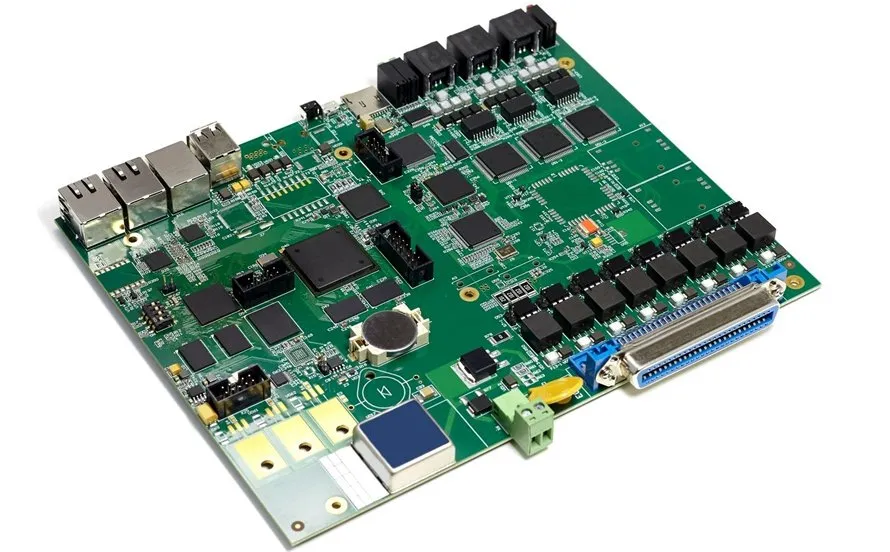
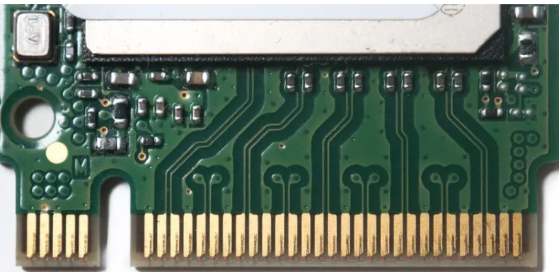
PCB edge plating is a specialized process that involves applying a metal coating to the exposed copper connections at the edge of a printed circuit board (PCB). This technique, also known as side plating, battlement, or metallized edge plating, enhances electrical connectivity, structural rigidity, and electromagnetic interference (EMI) shielding. This article provides an in-depth look at the...

Chip Scale Package Basics

Chip-Scale Package (CSP) is a type of integrated circuit packaging technology. The size of the package is up to 1.2 times the size of the actual die, with only a single-die and a direct surface mountable package. First originating in the 1990s, it was developed as a response to the demand for smaller and more efficient...

PCB Thermal Design Guide: Tips For PCB Analysis and Performance

Electronics are becoming faster, smaller, and used in more demanding environments. Miniaturized ICs and SMDs operate at higher frequencies and require more power. Increased current demands cause voltage drops across resistive elements, generating heat and leading to temperature rises and hotspots. Over half of electronic component failures now stem from heat-related stress. To develop high-quality circuit...

Common PCB Tolerances for Manufacturing

PCB tolerances for manufacturing refer to the allowable variations from specified dimensions, encompassing: material thickness, copper thickness, drilling, plating, and solder masks. These PCB tolerances ensure that PCB circuit boards are produced precisely and can function as intended. Manufacturers adhere to specific in-house tolerance guidelines, based on international standards like IPC-A-600 Class 2, to maintain quality throughout the...

The core control module of the wireless smart irrigation controller adopts a high-performance PCBA circuit board

Smart Water-Saving Irrigation Control System Solution Background Overview With the increasing global water scarcity, especially in large-scale agricultural planting areas, traditional irrigation methods face issues such as water waste, cumbersome manual operations, and imprecise irrigation control. To address these pain points, we have helped our customers develop a wireless smart irrigation controller PCBA. This controller utilizes...

Should You Use Plated or Unplated PCB Mounting Holes?

When designing a PCB, one of the critical decisions you’ll face is whether to use plated or unplated mounting holes. These holes are essential for securing the PCB to an enclosure or package, but the choice between plated and unplated holes depends on your design requirements, grounding needs, and mechanical considerations. Let’s explore the differences, advantages, and best...

Optimizing Small Wind Turbine Inverters: Enhancing Stability & Reliability

Optimizing Small Wind Turbine Inverters: Enhancing Stability & Reliability Customer Background & Market Demand Germany is a global leader in renewable energy, with its Energiewende (energy transition) policy driving widespread adoption of distributed wind power for rural electrification, industrial parks, and off-grid energy solutions. Small Wind Turbines (SWTs) have become an essential power supply option due to their flexibility...

KKPCB Case Study: High-Frequency Fiber Optic Transceiver PCB for Fiber Instrument Sales

1. Customer Profile Client:  Anonymous Industry: Fiber Optic Test & Measurement, High-Speed Data Transmission Application: Next-gen 100G/400G+ optical transceivers, OTDR equipment, and 50GHz RF test modules. FIS designs precision fiber optic tools, requiring ultra-low-loss PCBs to maintain signal integrity at millimeter-wave frequencies (up to 50GHz). Their challenges include: Insertion loss degrading high-speed signals (>40Gbps). Impedance mismatches causing reflection noise. Thermal expansion leading to microvia cracking in compact...

1. Customer Profile Client: Anonymous Industry: Telecom Infrastructure, 5G Macro/Micro Base Stations Application: Power Amplifier (PA) Modules + RF Front-End PCBs High-power base station equipment requiring PCBs are able to handle: High current (30A+) for PAs Low-loss RF (3.5GHz-28GHz for 5G) Thermal stability (85°C ambient, 125°C local hotspots) Key Challenges Faced: Delamination risk from mixed thick-copper (6oz) and RF layers. EMI...