
In PCB manufacturing and electronic assembly, ensuring the electrical connection reliability of integrated circuits (ICs) is essential for product performance and long-term stability.
IC continuity testing is a key verification method used to confirm whether electrical connections between IC pins, PCB traces, vias, and surrounding components are correctly established.
During PCB assembly, potential issues such as:
- Open circuits
- Soldering defects
- Poor electrical contact
- Broken traces
- Short circuits
can affect IC functionality and cause system failures.
By performing continuity testing, manufacturers can identify connection problems at an early stage, improving production yield and reducing troubleshooting costs.
1. What Is IC Continuity Testing?
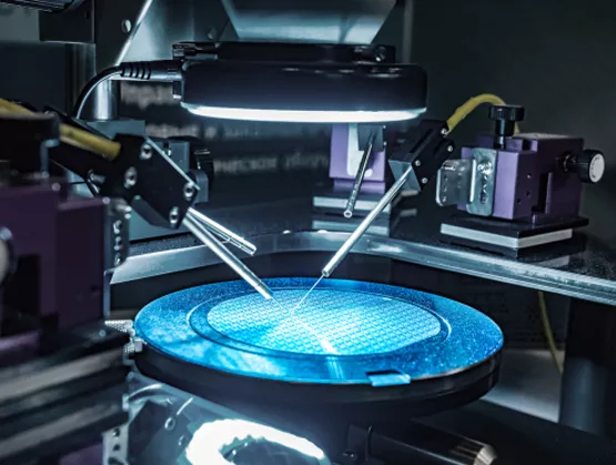
IC continuity testing is an electrical inspection method used to verify whether the conductive paths connected to an IC are continuous and electrically correct.
The test checks whether current can properly flow between:
- IC pins and PCB pads
- PCB traces
- Via structures
- Connected components
- Power and ground networks
The main purpose is to confirm:
- Correct electrical connections
- Stable signal paths
- Reliable solder joints
Unlike functional testing, continuity testing focuses primarily on the physical and electrical connection integrity of the circuit.
2. Why IC Continuity Testing Is Important
2.1 Detect Manufacturing Defects
During PCB assembly, defects may occur due to:
- Insufficient solder
- Solder bridging
- Component misalignment
- PCB fabrication errors
Continuity testing helps identify these issues before products enter final testing.
2.2 Improve Product Reliability
Poor IC connections may cause:
- Intermittent failures
- System instability
- Unexpected resets
- Communication errors
Early detection improves:
- Product lifetime
- Field reliability
- Customer satisfaction
2.3 Reduce Debugging Time
Without continuity testing, engineers may need to spend significant time diagnosing:
- Component failures
- Software problems
- Circuit design issues
Electrical verification helps quickly determine whether the problem originates from PCB connections.
3. Basic Principle of IC Continuity Testing
The basic principle is to apply a small electrical signal between two test points and measure whether the expected electrical path exists.
The testing system evaluates:
- Resistance value
- Electrical connection status
- Signal continuity
A normal connection typically shows:
- Low resistance
- Stable electrical conduction
A failed connection may show:
- Infinite resistance
- Unstable resistance
- Unexpected electrical paths
4. Common IC Continuity Testing Methods
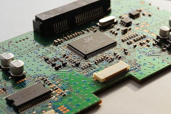
4.1 Multimeter Continuity Test
The simplest method uses a digital multimeter.
The instrument applies a small voltage and checks whether current flows.
Applications:
- Prototype boards
- Low-volume PCB verification
- Engineering debugging
Advantages:
- Simple operation
- Low cost
Limitations:
- Manual testing
- Limited test coverage
4.2 Flying Probe Testing
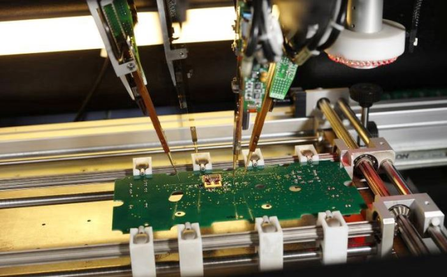
Flying probe testers use movable probes to contact PCB test points.
The system automatically checks:
- Open circuits
- Short circuits
- Connection resistance
Advantages:
- No custom fixture required
- Suitable for prototypes and small batches
- Flexible for design changes
Applications:
- Prototype PCB
- Low-volume production
4.3 In-Circuit Test (ICT)
ICT uses a dedicated fixture to test multiple points simultaneously.
It can verify:
- IC pin connections
- Passive components
- Power networks
- Signal paths
Advantages:
- High testing speed
- Suitable for mass production
Limitations:
- Requires test fixture development
- Higher initial cost
4.4 Boundary Scan Testing
Boundary scan technology uses built-in IC test functions.
Common standard:
- IEEE 1149.1 JTAG
It can test connections between IC devices without requiring physical access to every node.
Advantages:
- Suitable for high-density PCB designs
- Effective for BGA packages
- Supports complex digital systems
Applications:
- Communication boards
- Industrial controllers
- Advanced computing systems
5. Key Parameters in IC Continuity Testing
5.1 Resistance Measurement
Resistance is one of the main indicators.
A good connection usually has:
- Low resistance
- Stable measurement results
High resistance may indicate:
- Poor solder joint
- Damaged trace
- Contact problem
5.2 Test Current
The test current must be carefully controlled.
Excessive current may:
- Damage sensitive components
- Affect measurement accuracy
5.3 Test Point Accessibility
PCB design should consider testing requirements.
Good testability includes:
- Sufficient test points
- Clear probe access
- Proper spacing
6. PCB Design Considerations for IC Continuity Testing
6.1 Add Appropriate Test Points
During PCB layout, engineers should reserve test points for:
- Power rails
- Ground connections
- Important signal lines
- Communication interfaces
Benefits:
- Easier debugging
- Faster production testing
- Improved quality control
6.2 Consider BGA Package Testing
BGA packages create challenges because solder joints are hidden underneath the component.
Solutions include:
- Boundary scan testing
- X-ray inspection
- Dedicated test structures
6.3 Optimize Trace Routing
Reliable IC continuity requires:
- Proper trace width
- Stable via connections
- Correct layer transitions
Poor routing may cause:
- Signal interruption
- Manufacturing defects
7. Common IC Continuity Test Failures and Causes
7.1 Open Circuit Failure
Symptoms:
- No electrical connection
- System does not operate
Possible causes:
- Broken trace
- Missing solder
- Poor via connection
7.2 Short Circuit Failure
Symptoms:
- Unexpected current flow
- System malfunction
Possible causes:
- Solder bridging
- Incorrect PCB fabrication
- Contamination
7.3 High Resistance Connection
Symptoms:
- Intermittent operation
- Signal instability
Possible causes:
- Cold solder joint
- Oxidized surface
- Insufficient solder contact
8. Relationship Between Continuity Testing and PCB Assembly Quality
IC continuity testing is closely related to PCBA manufacturing quality.
A complete quality control process may include:
AOI Inspection
Detects:
- Component placement errors
- Visible solder defects
X-Ray Inspection
Used for:
- BGA solder joints
- Hidden connections
ICT Testing
Verifies:
- Electrical connectivity
- Component parameters
Functional Testing
Confirms:
- Actual product operation
Together, these methods provide comprehensive PCB assembly verification.
9. IC Continuity Testing in Different Applications
Consumer Electronics
Requirements:
- High production volume
- Fast testing speed
Automotive Electronics
Requirements:
- High reliability
- Long service life
Testing focuses on:
- Connection stability
- Environmental durability
Industrial Control Systems
Requirements:
- Continuous operation
- Strong resistance to interference
Medical Electronics
Requirements:
- High accuracy
- Strict reliability standards
10. How to Improve IC Continuity Test Efficiency
Improve PCB Testability
Design considerations:
- Add test points early
- Follow DFT (Design for Testability) principles
- Ensure probe accessibility
Combine Multiple Inspection Methods
A reliable production process combines:
- AOI
- ICT
- X-ray
- Functional testing
Perform DFM Review Before Manufacturing
DFM analysis helps identify:
- Difficult solder joints
- Testing limitations
- Assembly risks
before mass production.
Conclusion
IC continuity testing is an important part of PCB and PCBA quality control. It verifies that electrical connections between IC components and PCB structures are reliable and free from manufacturing defects.
By combining appropriate testing methods such as:
- Multimeter testing
- Flying probe testing
- ICT
- Boundary scan testing
manufacturers can improve production quality and reduce failures.
For high-density and high-performance electronic products, continuity testing should be considered during PCB design through proper test point planning, trace optimization, and DFT principles.
A well-designed PCB with effective continuity testing helps achieve higher reliability, faster production validation, and smoother transition from prototype development to mass production.
