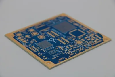
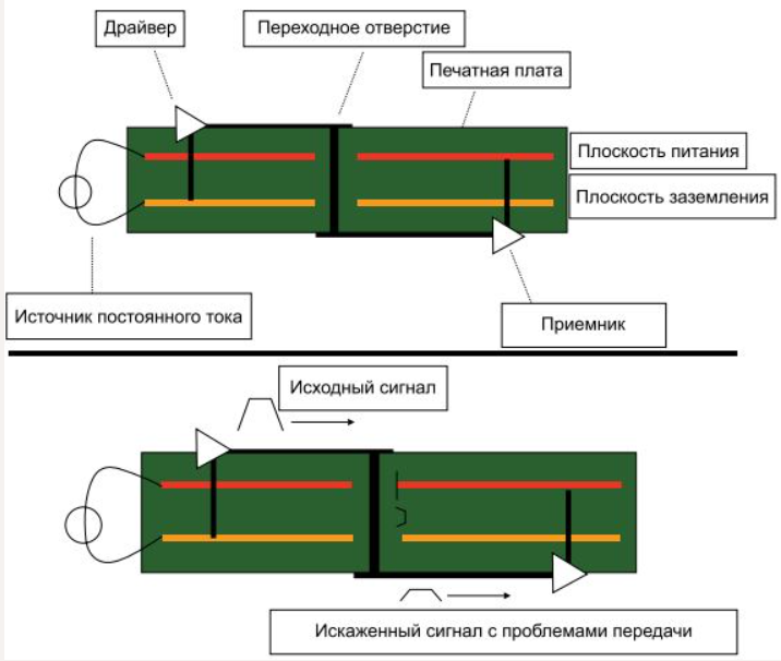
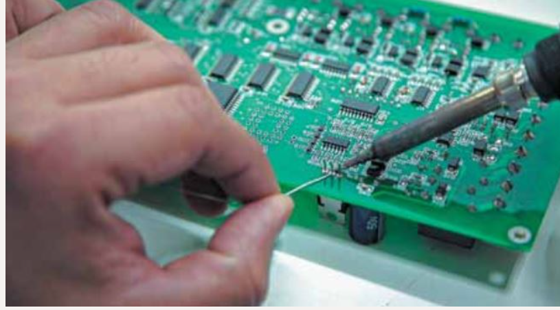
kkpcba-Cindy - KKPCB - Page 2 of 74
 
HomeAuthor

kkpcba-Cindy - KKPCB - Page 2 of 74

PCB Pad Soldering Processes Explained: Types, Features, and Selection Guide

Why PCB Pad Soldering Process Matters In PCB manufacturing, the pad surface finish or soldering process directly affects component solderability, electrical performance, and long-term reliability.Different processes offer varying degrees of oxidation resistance, flatness, and cost efficiency, making proper selection essential for every PCB design project. This article categorizes and compares the most common PCB pad...

Why Should Vias Be Staggered from Pad Positions in PCB Design?

 The Importance of Via Placement in PCB Design In PCB design, via positioning plays a crucial role in ensuring electrical performance, manufacturing reliability, and signal integrity. Improper via placement—especially placing vias directly on component pads—can lead to soldering defects, electrical noise, and higher production costs. This article explains why vias should be staggered from pad...

What are RSRP and RSRQ in 5G?

With the rapid development and widespread application of 5G technology, the field of wireless communication has ushered in unprecedented changes. In 5G networks, signal quality monitoring and evaluation are crucial for ensuring communication stability and reliability. Among them, Reference Signal Received Power (RSRP) and Reference Signal Received Quality (RSRQ) are two key performance indicators that play an...

Power supply noise is a common problem on high-frequency PCBs . This interference is usually caused by electromagnetic fields generated when current flows across the PCB. Electromagnetic fields are generated when current flows through power or ground lines on the PCB. If these fields interact with other components on the PCB, they can produce noise, thus affecting circuit performance....

SMT PCB Assembly Process – 8 Basic Steps

With the rapid development of today’s electronics industry, electronic products are becoming smaller, lighter, and more complex. To meet this demand, engineers have adopted Surface Mount Technology (SMT) — an advanced PCB assembly method that allows components to be mounted directly onto the surface of the printed circuit board. If you’ve ever looked at the...

PCB Design Best Practices: Key Considerations for Optimized Performance

When designing printed circuit boards (PCBs), a well-structured approach and attention to detail are essential to ensure functionality and avoid potential design errors. Here are some key PCB design tips based on practical experience: 1. Pay Attention to Pin Definitions and Package Names in the Schematic Library When creating the schematic library, ensure that each schematic pin corresponds correctly...

PCB Layout Best Practices: Essential Design Considerations for Reliable Electronic Products

PCB design translates electrical schematics into a functional product, and its quality directly impacts production efficiency and product reliability. For beginners, mastering PCB layout can be challenging despite familiarity with design software, and common issues often arise. Here, seasoned engineers from KKPCB share their PCB layout insights to help avoid these pitfalls and inspire best practices. Component Placement...

What are Thin and Thick Film Resistors?

Thin and Thick Film Resistors are the most common types in the market. They are characterized by a resistive layer on a ceramic base. Although their appearance might be very similar, their properties and manufacturing process are very different. The naming originates form the different layer thicknesses. Thin film has a thickness in the order of 0.1μm...