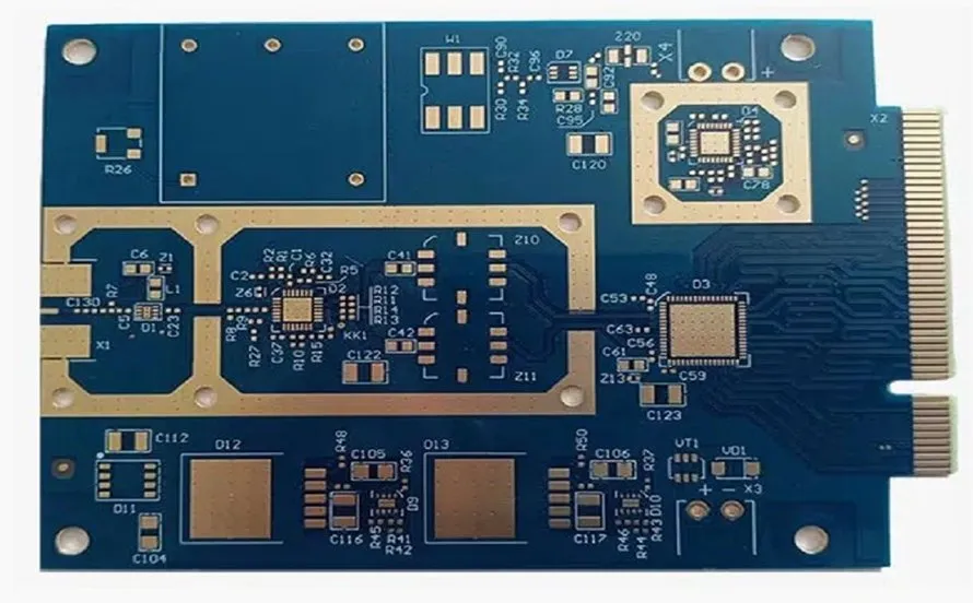
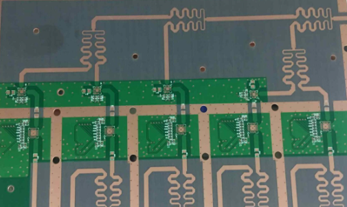
Engineering Context / Abstract The rapid deployment of 5G communication infrastructure has driven router and baseband system designs toward higher channel bandwidth, tighter phase tolerance, and increased RF integration density. In sub-6 GHz and emerging mmWave backhaul links, phase consistency across parallel RF paths directly impacts beamforming accuracy, MIMO synchronization, and overall system throughput....
HomeAuthor
kkpcba-Cindy - KKPCB
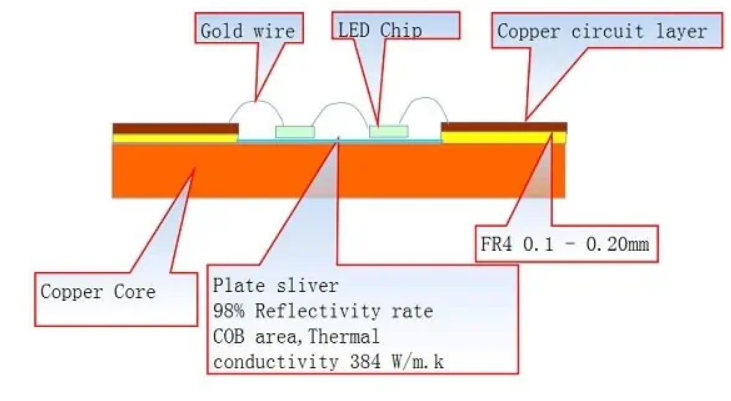
What Is a Multilayer Metal Core PCB? Multilayer Metal Core PCBs (MCPCBs) are advanced printed circuit boards that incorporate a metal core layer—such as aluminum, copper, or iron alloy—within a multilayer PCB structure. Compared with traditional FR4 multilayer PCBs, multilayer MCPCBs offer: Significantly enhanced thermal conductivity Superior heat dissipation Improved mechanical rigidity Higher power density...
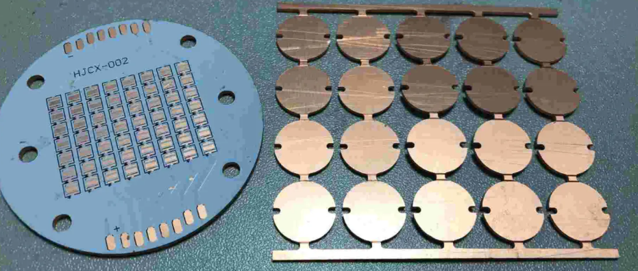
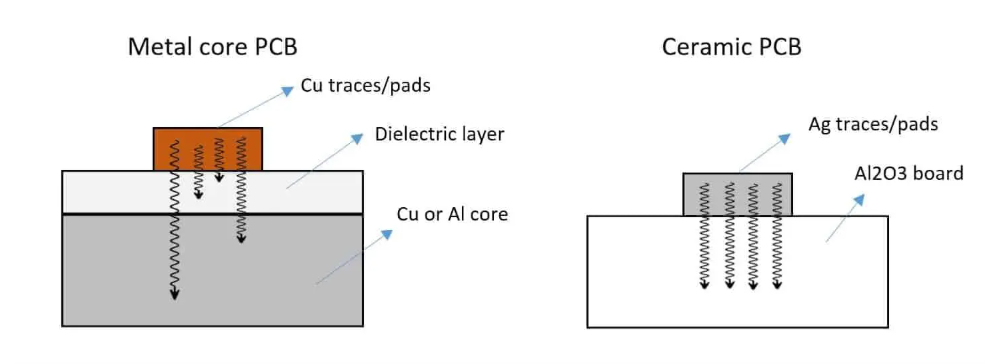
What Is a Metal Core PCB (MCPCB)? A Metal Core Printed Circuit Board (MCPCB) uses a metal substrate—typically aluminum, copper, or iron alloy—as the core layer instead of standard FR4 dielectric material. Thanks to the high thermal conductivity of metal substrates, MCPCBs can efficiently dissipate heat generated by high-power electronic components, making them essential for:...
1. Why Thermal Conductivity of Metals Matters in PCB Applications Metals are widely used in electronic devices and printed circuit boards (PCBs) due to their excellent electrical and thermal properties. However, not all metals conduct heat equally. High thermal conductivity metals rapidly transfer heat and are ideal for heat dissipation Low thermal conductivity metals restrict...
1. Why Heat Dissipation Has Become a Critical PCB Design Challenge With the rapid development of integrated circuits (ICs) and microelectronic packaging technologies, electronic systems are becoming: Smaller in physical size Higher in power density More integrated and compact As a result, heat flux density around electronic devices continues to rise sharply. Excessive heat accumulation...
Why PCB Thermal Conductivity Matters As power density and operating frequencies continue to increase, thermal management has become a critical factor in PCB design. Excessive heat can lead to signal degradation, reduced component lifespan, and even system failure. This article from KKPCB provides a technical comparison of PCB thermal conductivity across four commonly used substrate...
Rogers CuClad 6700 is a CTFE thermoplastic adhesive film with a low melting point, low dielectric constant, and excellent CTE compatibility, specifically designed for bonding PTFE-based laminates and stripline structures in multilayer RF and microwave PCBs. At KKPCB, Rogers CuClad 6700 is widely used in high-frequency multilayer PCB stack-ups, especially where PTFE substrates require reliable,...
Rogers RT/duroid 5880 is one of the most widely used microwave and millimeter-wave PCB substrates, known for its ultra-low dielectric loss and stable electrical performance. It is extensively applied in radar systems, satellite communications, 5G infrastructure, automotive radar, aerospace, and high-speed digital circuits. In this article, KKPCB provides a comprehensive technical overview of RT/duroid 5880,...
Why Photoresist Selection Matters in PCB Manufacturing Printed Circuit Boards (PCBs) are the foundation of all electronic products. Whether used in consumer electronics, automotive systems, or high-frequency RF applications, accurate circuit pattern transfer is critical to PCB performance and reliability. In PCB fabrication, photoresist films—commonly divided into dry film and wet film—play a key role...
1. Introduction to Rogers High-Frequency PCB Materials In RF, microwave, and high-speed communication applications, PCB material selection plays a decisive role in signal integrity, loss control, thermal stability, and long-term reliability. Rogers Corporation is a globally recognized supplier of high-frequency PCB laminates, widely used in: RF and microwave circuits Automotive radar 5G and millimeter-wave systems...

