kkpcb04 - KKPCB - Page 5 of 96
 
HomeAuthor

kkpcb04 - KKPCB - Page 5 of 96

Microvia PCBs: Enabling High-Density and High-Performance Electronics

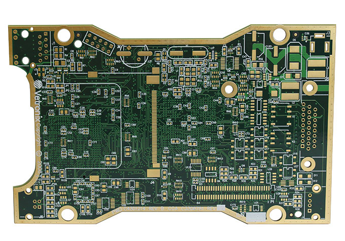
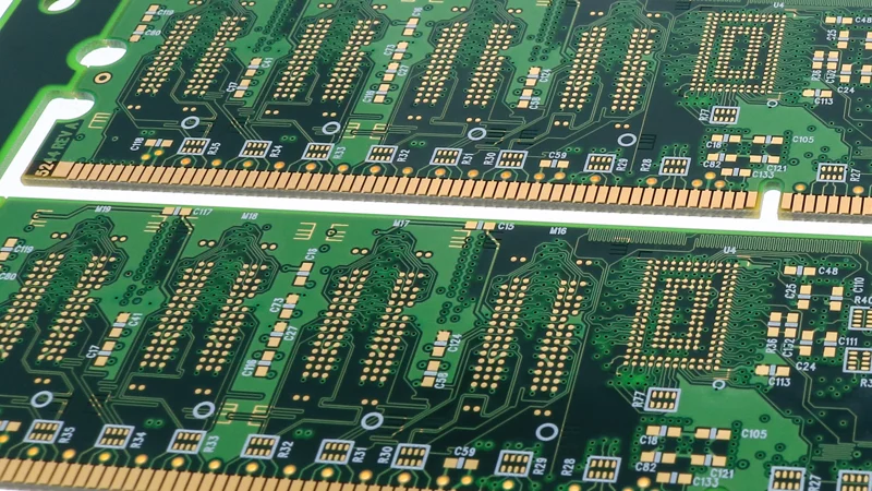
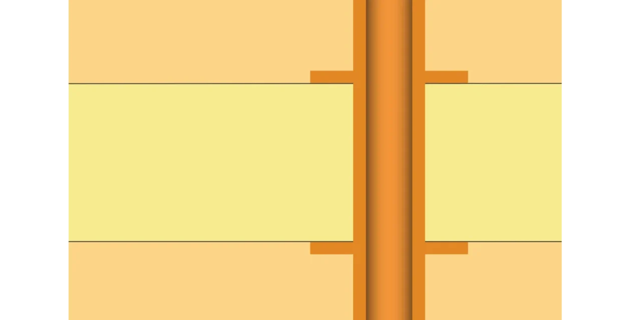
What is a Microvia PCB? A Microvia PCB is a printed circuit board that uses very small vias—typically less than 150 microns in diameter—to connect adjacent layers. Unlike traditional through-hole or buried vias, microvias enable high-density routing and reduced signal path lengths, making them ideal for high-speed, high-performance, and compact electronic designs. Microvia technology is...

High Reliability PCBs: Design, Manufacturing, and Applications

What is High Reliability PCB? High Reliability PCBs are designed to operate consistently in demanding environments where failure is not an option. These boards are used in aerospace, defense, medical devices, automotive, and industrial systems, where extreme conditions like high temperatures, vibration, humidity, and high-frequency operation can challenge standard PCBs. A High Reliability PCB focuses...

Fine Pitch PCBs: Precision Design for High-Density Components

As electronic devices become smaller and more powerful, the demand for Fine Pitch PCBs—boards designed for components with extremely small pin spacing—has grown significantly. Fine pitch components, such as BGA, QFN, and CSP packages, require precise PCB design and manufacturing to ensure electrical connectivity, signal integrity, and long-term reliability. Design Considerations High-Density Layouts:Fine pitch PCBs...

Low Loss PCBs: Optimizing Signal Integrity for High-Frequency Applications

In modern electronics, especially in RF, 5G, and high-speed communication systems, signal loss can significantly affect device performance. Low loss PCBs are specifically designed to minimize dielectric and conductor losses, ensuring high-frequency signals propagate with minimal attenuation. These PCBs are essential for applications such as mmWave modules, RF transceivers, antennas, and satellite communication systems. Design...

Custom ATE PCBs: Precision Design for Automated Test Equipment

Automated Test Equipment (ATE) plays a vital role in validating electronic components, modules, and systems. At the heart of these test platforms are Custom ATE PCBs, engineered to handle high-speed signals, precise routing, and repeated testing cycles without failure. These PCBs must balance electrical performance, mechanical stability, and long-term reliability to meet stringent testing requirements....

Multilayer Test PCBs: Ensuring Reliability in Complex Electronics

Multilayer PCBs are the backbone of modern electronics, from high-speed communication modules and industrial sensors to automotive and aerospace systems. Before committing to full-scale production, engineers rely on multilayer test PCBs to validate designs, assess signal integrity, and identify potential manufacturing challenges. These test boards simulate the full stack-up of the final product, allowing for...

HDI PCBs: Unlocking High-Density Performance for Modern Electronics

High-Density Interconnect (HDI) PCBs are a key technology for today’s compact and high-performance electronics. With fine lines, microvias, blind and buried vias, and multiple layers, HDI PCBs allow designers to fit complex circuits into small form factors, supporting applications from mobile devices to 5G infrastructure, automotive electronics, aerospace systems, and industrial IoT devices. Advanced Design...

Buried Via PCBs: Advanced Techniques for High-Density Multilayer Boards

Buried via technology has become essential in modern PCB design, particularly for high-density, high-performance applications. Unlike through-hole vias that pass through all layers, buried vias connect only internal layers, leaving outer layers uninterrupted. This allows designers to maximize routing space, improve signal integrity, and achieve compact, multilayer PCB layouts. Design Advantages Maximizing Board Real Estate:By...

High Layer Count PCBs: Design Challenges and Manufacturing Solutions

High Layer Count PCBs (printed circuit boards with 8 layers or more) have become a cornerstone in advanced electronics design. From telecommunications and medical devices to automotive and aerospace systems, these boards allow engineers to pack more functionality into smaller footprints while maintaining high performance. However, as layer counts increase, both design and manufacturing complexities...

Buried Via PCB: Advanced Multilayer Interconnects for High-Density Electronics

As electronic devices become smaller and more complex, the need for high-density interconnections within printed circuit boards increases. Buried via PCBs offer a solution by connecting inner layers without using surface space, allowing for compact, high-performance multilayer boards. Buried vias improve routing flexibility, signal integrity, and design density, making them critical for advanced applications such...