Customer CaseElectronics Industry NewsEngineering TechnologiesPCB DesignPCB ManufacturingPCB Materials
ENIG PCB Surface Finish: Benefits, Process, and Applications Explained
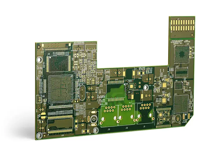
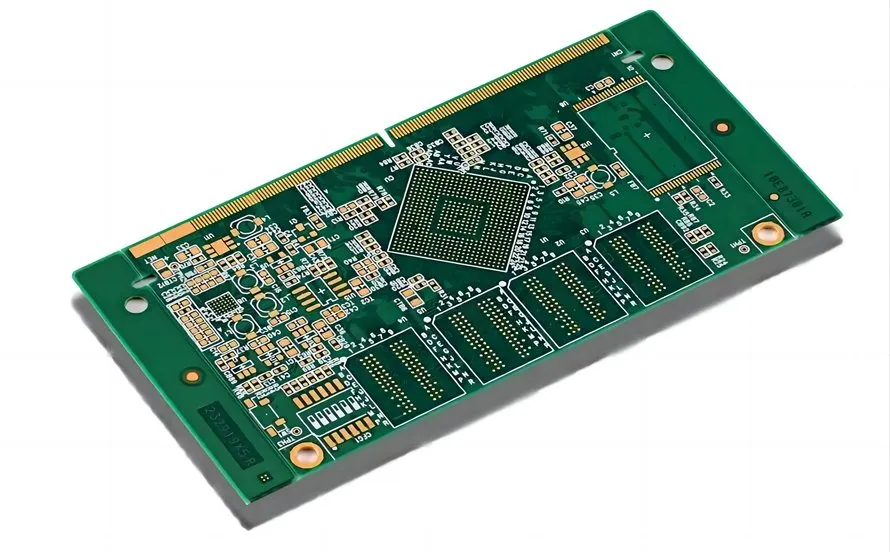
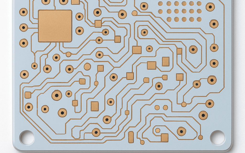
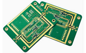
What Is ENIG PCB Surface Finish? What Is ENIG in PCB Manufacturing? ENIG (Electroless Nickel Immersion Gold) is one of the most widely used and highly reliable PCB surface finishes in the electronics industry. As a chemical deposition process, ENIG forms a two-layer metallic coating—a nickel barrier layer followed by a thin immersion gold layer—without...