KKPCB Blog – PCB & PCBA Insights, News, and Tips - KKPCB
 

Blog

Explore the KKPCB Blog for the latest PCB manufacturing and assembly news, industry insights, expert tips, and technology trends, helping you stay informed and optimize your electronics projects.
EPIG vs ENIG Solderability Performance After Steam Aging

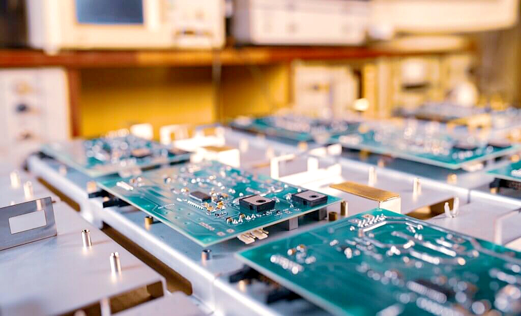
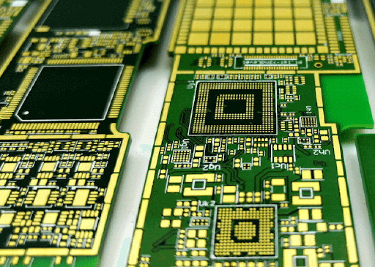
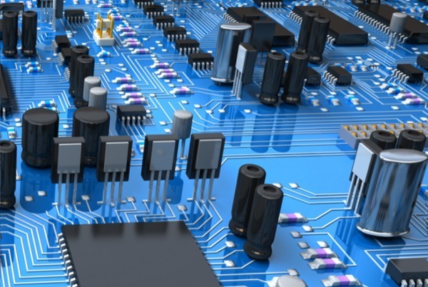
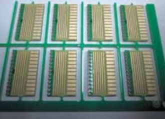
With the rapid development of high-frequency and high-reliability electronic products, the limitations of traditional ENIG (Electroless Nickel Immersion Gold) surface finishes have become increasingly evident. EPIG (Electroless Palladium Immersion Gold) has emerged as an advanced alternative, especially for RF, microwave, and fine-pitch PCB applications. This article, optimized and technically interpreted by KKPCB, presents a comparative...

PCB Turnkey Services: Streamlining Design, Manufacturing, and Assembly for Faster Time-to-Market

What Is PCB Turnkey? PCB Turnkey refers to a one-stop PCB solution where a single manufacturer manages the entire process—from bare PCB fabrication and electronic component procurement to assembly, testing, and logistics. Instead of coordinating multiple suppliers, customers work with one partner who takes full responsibility for quality, schedule, and delivery. At KKPCB, PCB Turnkey...

From Stackup Planning to Lamination Control: Engineering High Layer Count PCBs That Actually Work

Engineering High Layer Count PCBs: Why “More Layers” Isn’t the Answer As electronic systems evolve toward higher speeds, higher integration, and smaller form factors, high layer count PCBs—typically 16 layers and above—have become standard in data centers, telecommunications, aerospace electronics, and advanced industrial systems. However, many multilayer PCBs fail not because of schematic errors, but...

Balancing Electrical Performance and Manufacturability in Buried Via PCB Structures

As electronic systems continue to evolve toward higher speeds, greater functionality, and reduced form factors, Buried Via PCB structures have become a critical enabler for advanced multilayer designs. By allowing interlayer connections without penetrating the outer layers, buried vias unlock higher routing density, improved signal integrity, and enhanced EMI control. However, these electrical advantages must...

Designing High Layer Count PCBs for Complex Signal, Power, and Thermal Integrity Challenges

As electronic systems continue to integrate higher data rates, greater power density, and tighter form factors, high layer count PCBs have become a foundational platform for modern hardware architecture. Designs exceeding 16, 20, or even 30 layers are now common in data center equipment, telecommunications infrastructure, aerospace electronics, and industrial control systems. However, increasing layer...

Rigid-Flex PCB Engineering for Space-Saving, High-Reliability Electronic Systems

Rigid-Flex PCB as a System-Level Interconnect Architecture Rigid-Flex PCB technology integrates rigid PCB structures and flexible circuits into a single, unified interconnect platform. Compared with traditional rigid PCB assemblies connected by cables or connectors, a Rigid-Flex PCB significantly reduces interconnect interfaces while improving electrical continuity and mechanical robustness. In modern electronic systems, Rigid-Flex PCB designs...

Small Batch PCB Manufacturing for High-Mix, Engineering-Driven Electronics Development

Small Batch PCB manufacturing refers to low-volume PCB production typically ranging from a few pieces to several hundred units, designed to support prototype validation, pilot runs, and early-stage product commercialization. Unlike mass production, Small Batch PCB emphasizes engineering accuracy, process flexibility, and rapid iteration over scale efficiency. For modern electronics development, Small Batch PCB is...

PCB Turnkey Solutions for Integrated Design, Fabrication, Assembly, and Supply Chain Management

PCB Turnkey: A Complete Engineering-Driven Manufacturing Model PCB Turnkey refers to a fully integrated manufacturing solution that covers PCB fabrication, component sourcing, PCB assembly, functional testing, and logistics delivery under a single engineering-managed workflow. Unlike fragmented outsourcing models, PCB Turnkey services eliminate interface risk between suppliers and significantly improve quality consistency, lead time predictability, and...

Controlled Impedance PCB Engineering for High-Speed Digital and High-Frequency RF Applications

A Controlled Impedance PCB is a critical foundation for modern high-speed digital systems and high-frequency RF applications. As signal rise times shrink and operating frequencies extend into multi-GHz ranges, PCB interconnects must behave as predictable transmission lines rather than simple copper connections. Controlled Impedance PCB design ensures signal integrity, phase stability, and EMI compliance across...

Enable Ultra-High Interconnect Density and Signal Integrity with Advanced High Layer Count PCB Architectures

High Layer Count PCB: The Backbone of Complex Electronic Systems A High Layer Count PCB refers to a multilayer printed circuit board typically featuring 16 layers, 24 layers, 32 layers, or more, designed to support complex signal routing, dense interconnections, and advanced power distribution. As electronic systems continue to integrate higher data rates, tighter form...