Customer CaseElectronics Industry NewsEngineering TechnologiesPCB DesignPCB ManufacturingPCB Materials
Microwave IC Test PCB: Precision PCBs for High-Frequency and mmWave Semiconductor Testing
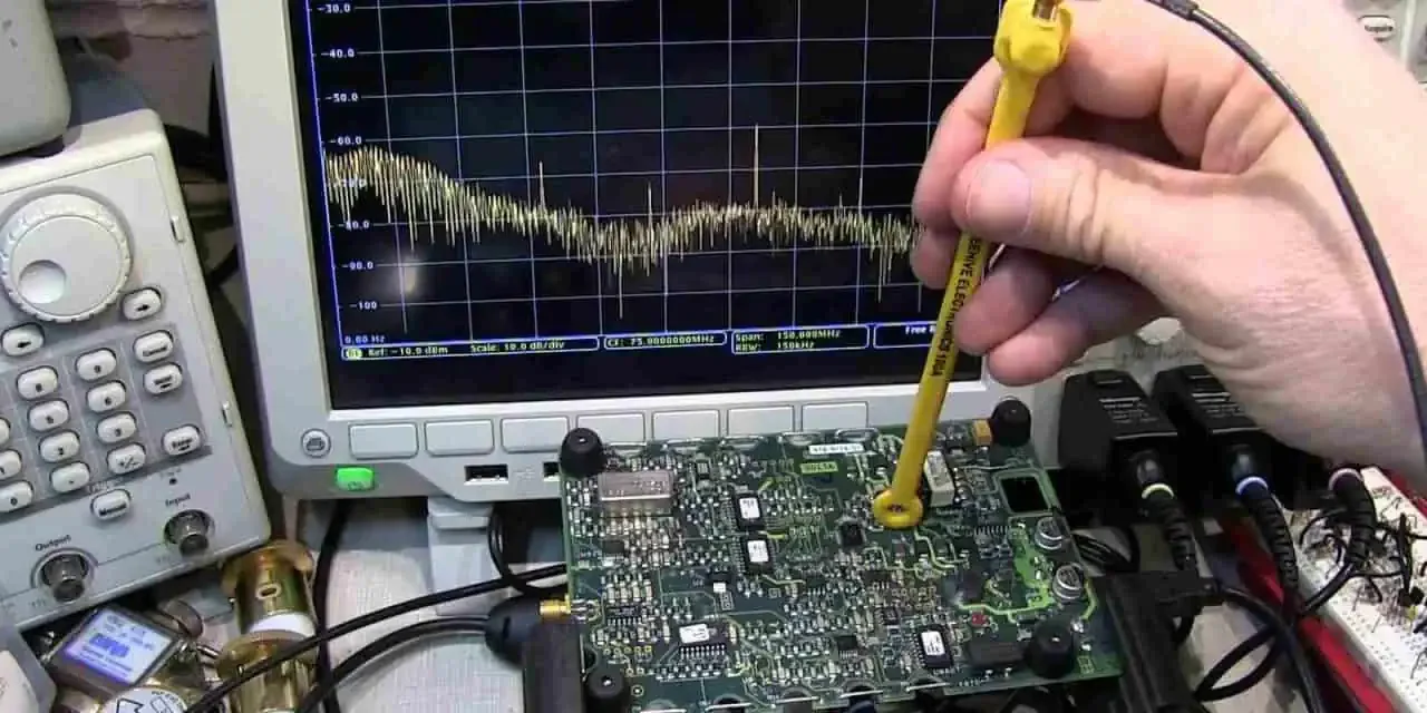
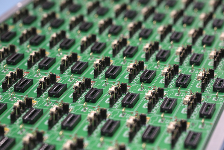
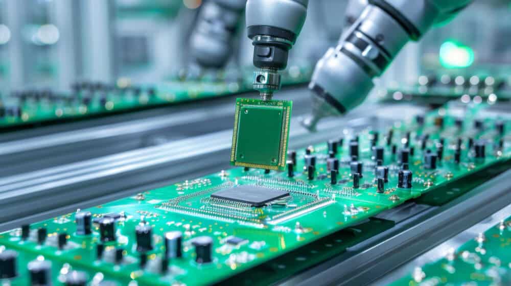
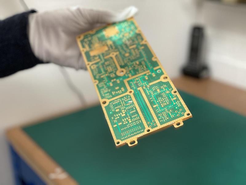
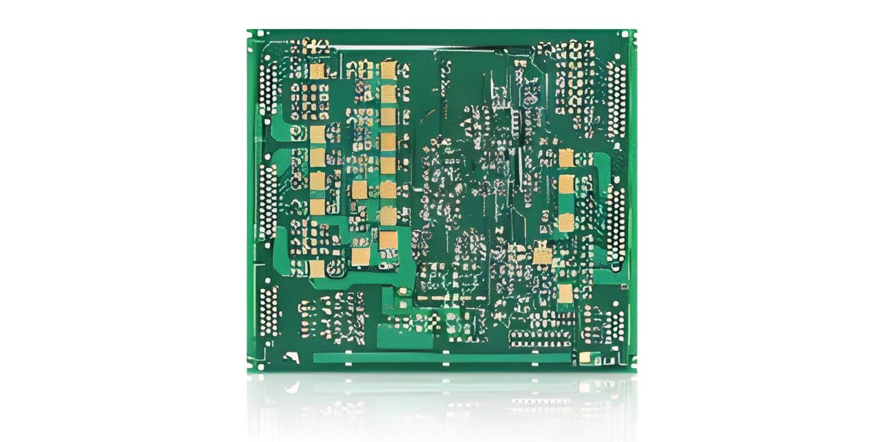
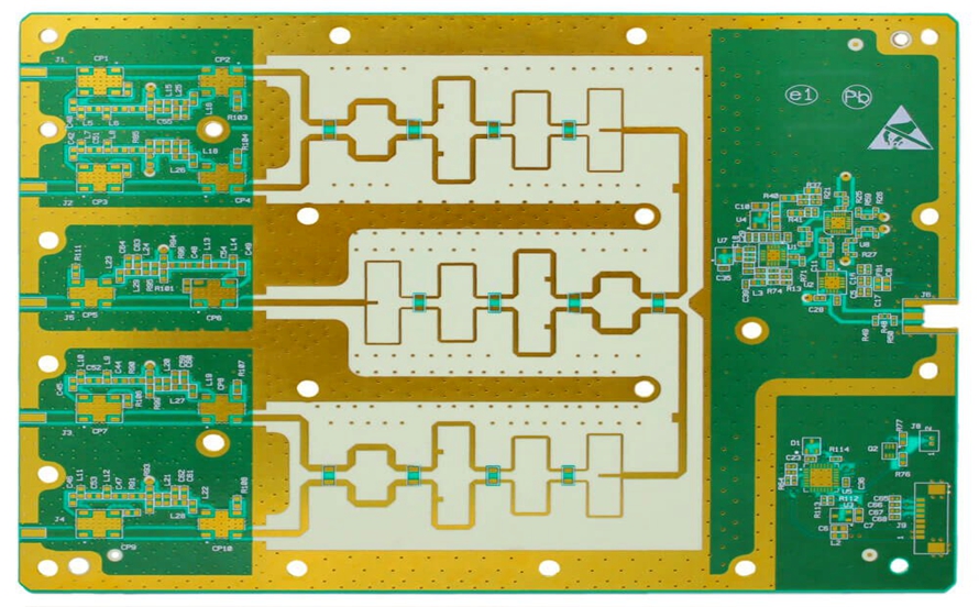
As semiconductor technology advances into microwave and mmWave frequency bands, accurate and repeatable testing becomes increasingly challenging. Microwave IC Test PCBs are specifically engineered to support high-frequency signal integrity, low insertion loss, and precise mechanical alignment, making them essential for validating microwave ICs used in 5G, radar, satellite communication, and high-speed wireless systems. A professionally...