KKPCB Blog – PCB & PCBA Insights, News, and Tips - KKPCB
 

Blog

Explore the KKPCB Blog for the latest PCB manufacturing and assembly news, industry insights, expert tips, and technology trends, helping you stay informed and optimize your electronics projects.
Accelerate Product Validation and Engineering Iteration with High-Reliability Small Batch PCB Manufacturing

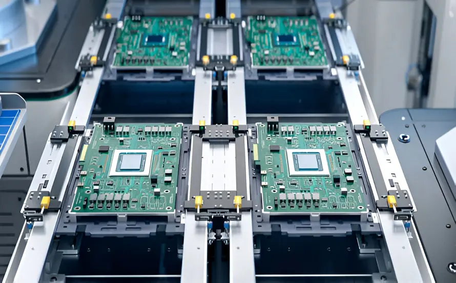
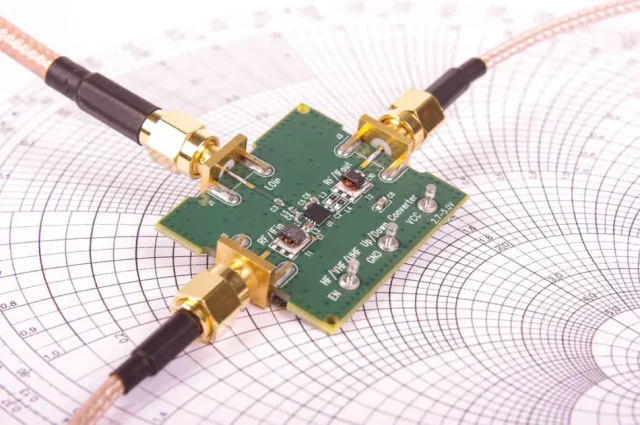
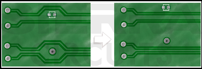
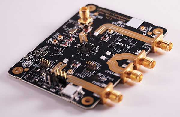
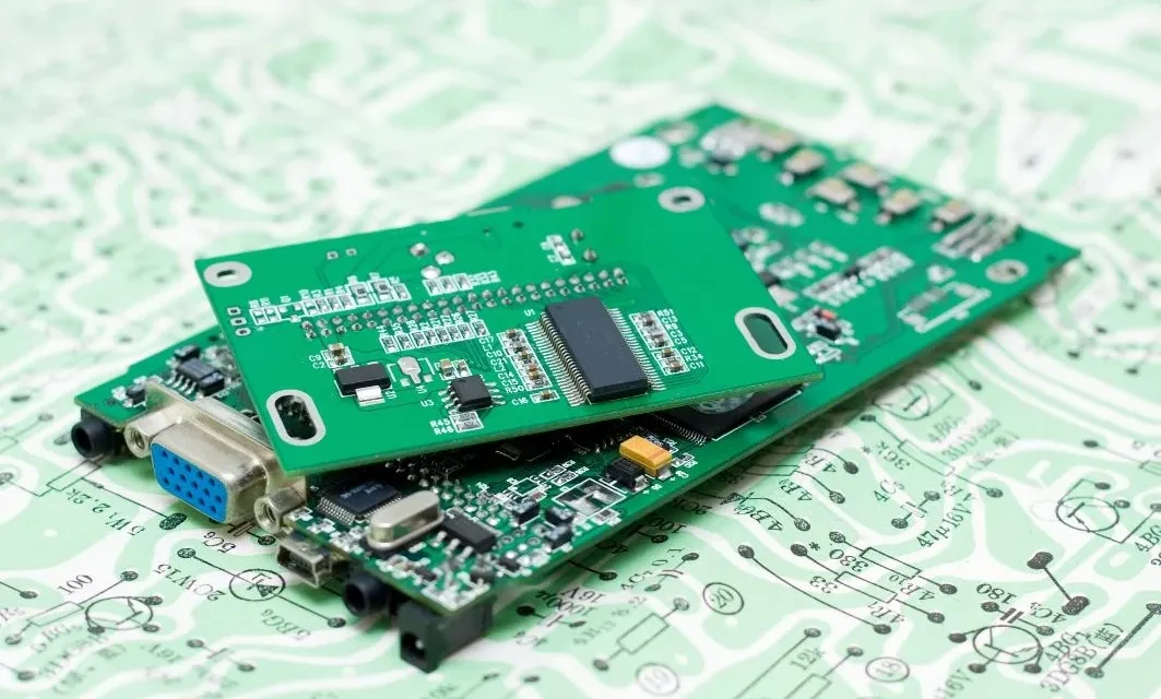
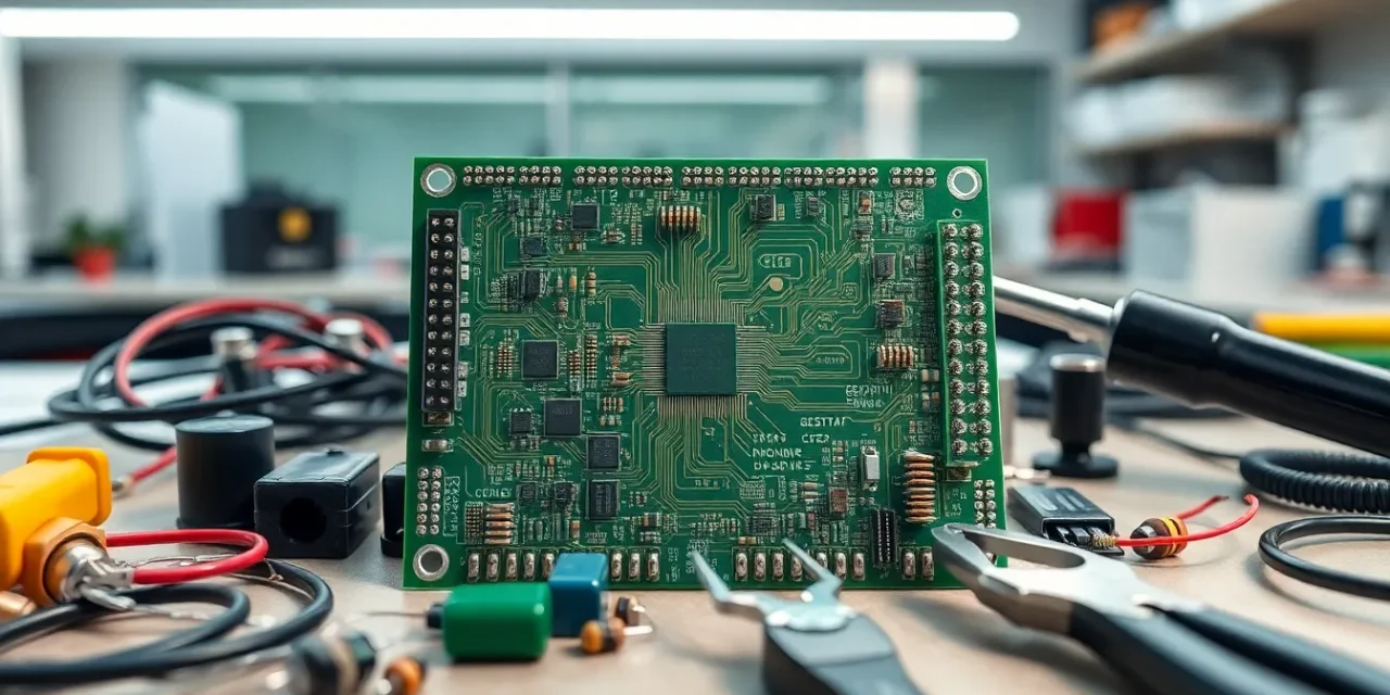
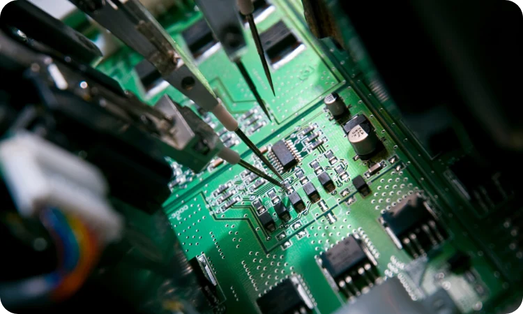
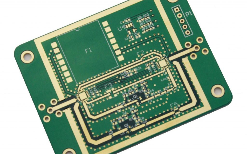
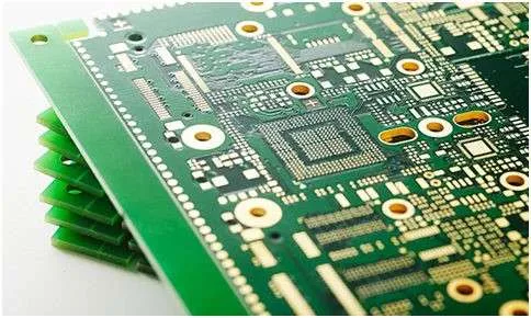
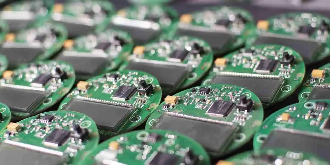
In today’s highly competitive electronics market, speed and reliability are critical during the product development stage. High-reliability small batch PCB manufacturing enables engineers to accelerate product validation, shorten engineering iteration cycles, and reduce development risk before mass production. This article explains how small batch PCB manufacturing supports rapid prototyping, design verification, and engineering optimization, helping...

PCB Turnkey Services: A Complete One-Stop Solution for PCB Manufacturing and Assembly

PCB Turnkey Services: A Complete One-Stop Solution for PCB Manufacturing and Assembly In today’s fast-paced electronics industry, reducing supply chain complexity and accelerating time to market are critical for success. PCB Turnkey services provide a complete, one-stop solution that covers every stage of electronics production—from PCB fabrication and component sourcing to assembly, testing, and final...

Impedance Control on PCBs: Why It Matters for High-Speed, RF, and High-Frequency Circuit Design

As electronic devices continue to evolve toward higher speeds, greater bandwidth, and higher operating frequencies, impedance control on PCBs has become a critical requirement rather than an optional design consideration. In high-speed PCB, RF PCB, and high-frequency circuit design, improper impedance control can lead to signal degradation, EMI issues, and overall system instability. This article...

Key Manufacturing Factors That Affect Controlled Impedance PCB Accuracy

Key Manufacturing Factors That Affect Controlled Impedance PCB Accuracy In today’s high-speed electronics market, Controlled Impedance PCB manufacturing has become a fundamental requirement for ensuring excellent signal integrity and stable electrical performance. As operating frequencies and data transmission speeds continue to rise, even minor impedance deviations in a controlled impedance PCB can result in signal...

Buy High Frequency PCBs Optimized for Controlled Impedance and Low Insertion Loss in 5G and Satellite Systems

As 5G wireless infrastructure and satellite communication systems continue to evolve toward higher frequencies, wider bandwidths, and denser integration, the demand to buy high frequency PCBs with precise electrical control has increased significantly. In these applications, controlled impedance PCB design and ultra-low insertion loss PCB performance are no longer optional—they are fundamental to achieving stable...

Designing Buried Via PCBs for High-Density Routing and Signal Integrity Optimization

As electronic systems continue to evolve toward higher speed, smaller form factors, and increased functionality, traditional through-hole via structures are becoming a limiting factor. Buried Via PCB technology has emerged as a critical enabler for high-density routing and signal integrity optimization, particularly in HDI, high-speed digital, and RF applications. By embedding vias between inner layers...

Small Batch PCB Manufacturing: Enabling Flexible Engineering Validation and Low-Risk Product Development

Why Small Batch PCB Matters in Modern Electronics Development In today’s electronics industry, product lifecycles are shorter and design iterations are more frequent. Before committing to mass production, engineering teams must validate signal integrity, power stability, thermal behavior, and manufacturability. Small batch PCB manufacturing plays a critical role in this phase by enabling controlled, low-risk...

PCB Turnkey Solutions: Streamlining Electronics Manufacturing from Design to Finished Assembly

Why PCB Turnkey Matters in Modern Electronics Manufacturing As electronic systems become more complex, managing separate suppliers for PCB fabrication, component sourcing, assembly, and testing introduces cost risk, schedule delays, and quality uncertainty. This is especially true for products involving high-speed digital signals, RF circuits, power electronics, or mixed-technology assemblies. PCB turnkey solutions address this...

Building Reliable High-Speed Electronics with Controlled Impedance PCB Architectures

Introduction: Why Controlled Impedance Defines High-Speed Reliability As high-speed electronics push into multi-gigabit data rates and high-frequency RF domains, signal behavior is no longer dominated by logic thresholds—it is governed by transmission line physics. In these systems, every PCB trace behaves as a controlled impedance structure, and any deviation can introduce reflections, timing skew, and...

Balancing Electrical Performance and Manufacturability in Buried Via PCB Structures

Balancing Electrical Performance and Manufacturability in Buried Via PCB Structures Buried vias are often introduced into PCB designs to improve electrical performance.Shorter signal paths, reduced stub effects, and higher routing density make buried via PCB structures attractive for high-speed and high-density applications. In practice, however, electrical optimization and manufacturing stability do not always move in...