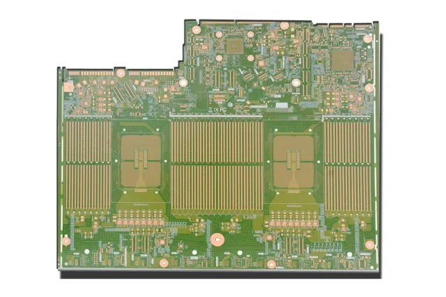
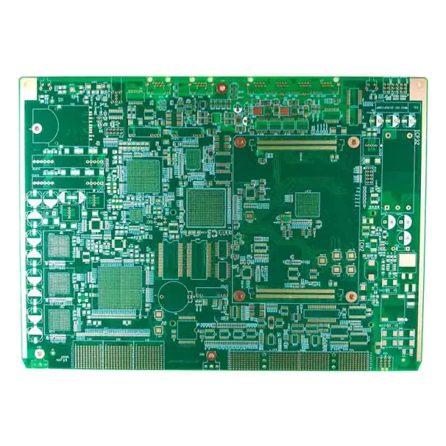
1. Introduction to Multilayer HF PCB Technology
As modern electronic systems continue evolving toward:
- Higher operating frequencies
- Faster data transmission
- Higher circuit density
- More compact device structures
traditional PCB technologies face increasing limitations in:
- Signal loss
- EMI control
- Thermal reliability
- High-speed signal transmission
To meet the requirements of:
- 5G communication systems
- Radar electronics
- Satellite communication
- Aerospace RF systems
- High-speed networking equipment
engineers increasingly rely on Multilayer HF PCB technology.
A Multilayer High-Frequency PCB (HF PCB) combines:
- High-frequency laminate materials
- Controlled impedance routing
- Multilayer stack-up optimization
- Advanced RF PCB manufacturing techniques
At KKPCB, multilayer HF PCB solutions are optimized for:
- Ultra-low signal loss
- Stable RF transmission
- High-reliability electronic systems
2. What Is a Multilayer HF PCB?
A Multilayer HF PCB is a multilayer printed circuit board specifically designed for:
- High-frequency RF signals
- Microwave circuits
- High-speed digital transmission
These PCBs typically use:
- Rogers laminates
- PTFE materials
- Low-loss dielectric substrates
to ensure:
- Stable impedance
- Low insertion loss
- Excellent signal integrity
3. Key Characteristics of Multilayer HF PCB
3.1 Low Signal Loss
High-frequency PCB materials feature:
- Low dielectric constant (Dk)
- Low loss tangent (Df)
Loss tangent is represented by:
tanδ\tan\deltatanδ
Low dielectric loss ensures:
- Reduced signal attenuation
- Improved RF efficiency
- Better high-frequency performance
3.2 Controlled Impedance Routing
Accurate impedance control improves:
- Signal integrity
- RF matching performance
- High-speed data stability
3.3 Excellent EMI Shielding
Multilayer structures provide:
- Dedicated ground planes
- Shielding layers
- Reduced electromagnetic interference
3.4 High Thermal Reliability
HF PCBs often operate in:
- High-power RF systems
- Continuous transmission environments
requiring:
- Efficient thermal dissipation
- Stable long-term reliability
4. Common Materials Used in Multilayer HF PCB
Popular high-frequency PCB materials include:
- Rogers RO4350B
- Rogers RT/duroid® 5880
- RO4003C
- Taconic RF materials
- PTFE-based laminates
These materials provide:
- Stable dielectric properties
- Low insertion loss
- Excellent RF performance
5. Multilayer Stack-Up Design for HF PCB
A well-designed multilayer stack-up improves:
- Signal return paths
- Impedance consistency
- EMI suppression
Typical stack-up considerations:
- Symmetrical layer structures
- Dedicated RF ground planes
- Controlled dielectric thickness
At KKPCB, stack-up engineering is optimized for:
- RF signal integrity
- Stable multilayer lamination
- Low-loss transmission performance
6. Signal Integrity Optimization in HF PCB Design
Signal integrity challenges increase at high frequencies due to:
- Reflection
- Crosstalk
- Insertion loss
- Impedance discontinuity
Best practices include:
- Short RF routing paths
- Smooth trace transitions
- Proper differential pair routing
- Ground via stitching
7. Thermal Management in Multilayer HF PCB
High-frequency power modules generate significant heat.
Thermal design techniques include:
- Thermal via arrays
- Copper heat-spreading planes
- Metal-backed structures
- High thermal conductivity materials
Proper thermal management improves:
- RF stability
- Power handling capability
- Product reliability
8. Manufacturing Challenges of Multilayer HF PCB
HF PCB fabrication requires:
- Precision lamination control
- Accurate drilling and plating
- Tight impedance tolerance
- Low-profile copper processing
Common manufacturing challenges:
- PTFE material handling
- Layer registration accuracy
- Controlled dielectric thickness
- Copper roughness optimization
9. HF PCB Testing and Quality Assurance
Advanced testing ensures:
- Stable impedance performance
- Reliable RF transmission
- Manufacturing consistency
Testing methods include:
- TDR impedance testing
- Network analyzer testing
- AOI inspection
- X-ray inspection
At KKPCB, advanced quality systems ensure:
- High-frequency performance consistency
- Reliable multilayer PCB production
10. Applications of Multilayer HF PCB
Multilayer HF PCBs are widely used in:
- 5G base stations
- RF amplifiers
- Automotive radar systems
- Aerospace communication equipment
- Satellite communication systems
- Microwave antennas
These applications require:
- High-frequency stability
- Low transmission loss
- Excellent EMI performance
11. Future Trends in Multilayer HF PCB Technology
Future developments focus on:
- mmWave communication
- AI data center networking
- Advanced radar systems
- Ultra-low-loss PCB materials
Emerging technologies include:
- Hybrid multilayer stack-ups
- Embedded RF components
- Ultra-thin dielectric structures
- Advanced thermal management systems
12. Conclusion
Multilayer HF PCB technology is essential for modern:
- RF communication systems
- Microwave electronics
- High-speed digital applications
By combining:
- Low-loss materials
- Controlled impedance design
- Advanced multilayer stack-up engineering
- Precision manufacturing
engineers can achieve:
- Superior signal integrity
- Stable RF performance
- Long-term thermal reliability
With extensive expertise in RF PCB manufacturing, KKPCB provides advanced multilayer HF PCB solutions for next-generation electronic systems.
