1. Introduction: Why Heavy Copper PCB Matters in Power Electronics
As modern electronic systems evolve toward:
- Higher current density
- Increased power conversion efficiency
- More compact power modules
- Higher thermal loads
standard PCB copper thickness is often insufficient for reliable operation.
In applications such as:
- Power supplies
- Electric vehicles (EV)
- Battery management systems (BMS)
- Industrial motor drives
- Renewable energy inverters
Heavy Copper PCB technology has become essential for ensuring stable current carrying capability and thermal reliability.
At KKPCB, heavy copper PCB solutions are engineered for high current, high thermal load, and long-term reliability applications.
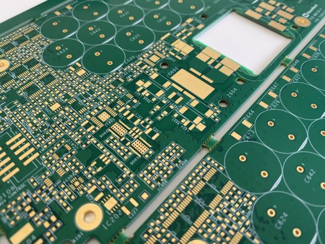
2. What Is a Heavy Copper PCB?
A Heavy Copper PCB is a printed circuit board that uses significantly thicker copper layers than standard PCBs.
Typical copper thickness:
- Standard PCB: 0.5 oz – 2 oz
- Heavy Copper PCB: 3 oz – 20 oz+
These thick copper structures enable:
- High current transmission
- Improved thermal dissipation
- Enhanced mechanical strength
3. Why Heavy Copper PCB Is Needed
3.1 High Current Carrying Capability
Heavy copper traces can handle large currents without overheating or failure.
Reducing resistance through thicker copper helps:
- Lower heat generation
- Improve efficiency
- Increase safety margin
3.2 Enhanced Thermal Management
Heavy copper layers act as:
- Heat spreaders
- Thermal conduction paths
This improves:
- Temperature uniformity
- Device reliability
- System lifespan
3.3 Improved Mechanical Strength
Thick copper increases:
- PCB structural rigidity
- Resistance to thermal stress
- Durability under vibration
4. Heavy Copper PCB Manufacturing Process
4.1 Copper Plating Process
Heavy copper is formed through:
- Electroplating multiple copper layers
- Controlled thickness deposition
4.2 Etching and Pattern Control
Challenges include:
- Maintaining trace geometry
- Preventing undercutting
- Ensuring dimensional accuracy
4.3 Multilayer Lamination
Heavy copper PCBs often require:
- High-pressure lamination
- Controlled thermal cycles
- Specialized resin systems
4.4 Drilling and Via Reliability
Due to thick copper:
- Drill wear increases
- Via plating requires reinforcement
At KKPCB, advanced processing ensures:
- Stable copper thickness control
- Reliable multilayer structure
- High current performance consistency
5. Thermal Performance of Heavy Copper PCB
Heavy copper significantly improves:
- Heat spreading efficiency
- Thermal conductivity
- Power density capability
Thermal management is critical in high-power systems where:
- Heat accumulation can reduce efficiency
- Excess temperature affects reliability
Solutions include:
- Copper plane optimization
- Thermal via arrays
- Metal-core hybrid structures
6. Electrical Performance and Current Density Design
Heavy copper PCB design must consider:
- Trace width
- Copper thickness
- Current distribution
Uniform current flow improves:
- System stability
- Reduced hot spots
- Better long-term reliability
7. Design Considerations for Heavy Copper PCB
7.1 Trace Geometry Optimization
Design must balance:
- High current capability
- PCB space constraints
- Thermal distribution
7.2 Layer Stack-Up Design
Proper stack-up improves:
- Heat dissipation
- Mechanical stability
- Electrical isolation
7.3 Via Reinforcement
Techniques include:
- Via filling
- Stacked vias
- Copper plating reinforcement
8. Manufacturing Challenges of Heavy Copper PCB
8.1 Etching Difficulty
Thicker copper increases:
- Etching complexity
- Edge profile variation risk
8.2 Layer Alignment Issues
Heavy copper requires:
- High-precision lamination
- Tight registration control
8.3 Cost and Processing Time
Compared to standard PCBs:
- Higher material cost
- More complex processing steps
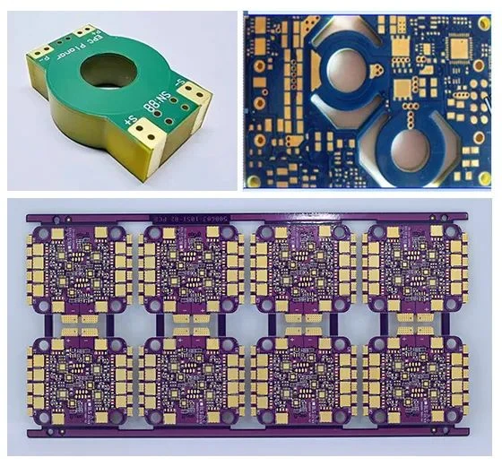
9. Applications of Heavy Copper PCB
Heavy Copper PCBs are widely used in:
- Electric vehicle power systems
- Battery management systems (BMS)
- Industrial power converters
- Solar inverters
- Motor control systems
- High-power LED drivers
These applications require:
- High current handling
- Thermal stability
- Long operational life
10. Future Trends in Heavy Copper PCB Technology
Future developments include:
- Hybrid heavy copper + HDI structures
- Advanced thermal composite materials
- Higher current density designs
- Integration with power modules
Heavy copper PCB will continue evolving to support:
- Electrification of transportation
- Renewable energy systems
- High-efficiency industrial electronics
11. Conclusion
Heavy Copper PCB technology is essential for modern high-power electronic systems requiring:
- High current capacity
- Excellent thermal performance
- Strong mechanical reliability
Through optimized copper thickness design and advanced manufacturing control, engineers can achieve:
- Stable power transmission
- Reduced thermal stress
- Long-term system reliability
With deep expertise in power electronics manufacturing, KKPCB delivers high-performance PCB solutions for demanding industrial and automotive applications.
