HomeTag

Multilayer Test PCB - KKPCB

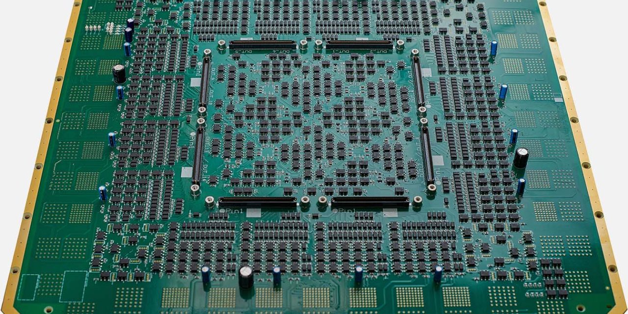
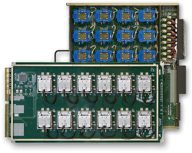
Burn-in Board PCB for Semiconductor Reliability and Stress Testing

What Is a Burn-in Board PCB? A Burn-in Board PCB is a specialized printed circuit board used in semiconductor reliability testing to identify early device failures. It connects packaged integrated circuits to burn-in test systems, allowing devices to operate under elevated temperature, voltage, and electrical stress conditions over extended periods. Burn-in board PCBs play a...
Semiconductor Load Board for IC Testing and Automated Test Equipment

What Is a Semiconductor Load Board? A Semiconductor Load Board is a critical interface PCB used in IC testing systems, connecting the automated test equipment (ATE) to the device under test (DUT). It provides electrical routing, signal conditioning, power delivery, and mechanical support during functional, parametric, and performance testing of semiconductor devices. Load boards are...

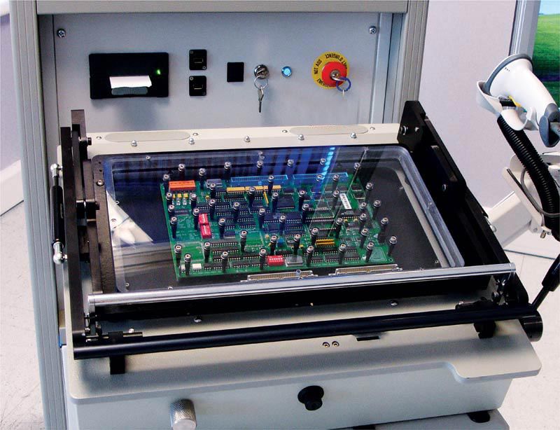
Automated Test Equipment PCB Manufacturing for High-Speed and High-Reliability Semiconductor Testing

In modern semiconductor manufacturing, Automated Test Equipment (ATE) plays a critical role in verifying the performance, reliability, and functionality of integrated circuits. At the core of every ATE system is the Automated Test Equipment PCB, which serves as the electrical interface between the test system and the device under test (DUT). An ATE PCB must...

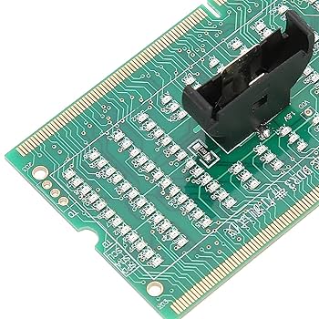
Memory Test PCB Manufacturing for DRAM, NAND and High-Speed Memory Testing

As memory devices continue to evolve toward higher speed, higher density, and lower power consumption, precise testing becomes increasingly critical. A well-designed Memory Test PCB is essential for validating the performance, reliability, and functionality of DRAM, NAND Flash, and other memory ICs throughout development and production stages. Memory test PCBs provide the electrical interface between...

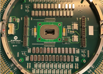
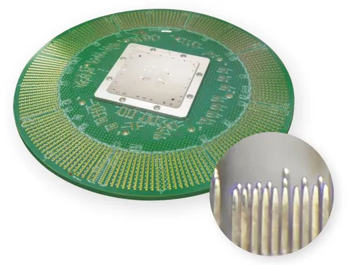
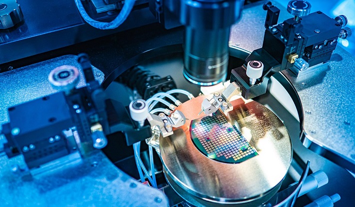
Wafer Test PCB Manufacturing for Accurate Semiconductor Wafer Testing

In semiconductor manufacturing, wafer testing is a critical step performed before packaging to verify die functionality and performance. A high-quality Wafer Test PCB serves as the electrical interface between the wafer probe card and automated test equipment (ATE), enabling precise signal transmission and accurate measurement results. As IC designs continue to scale in speed, density,...

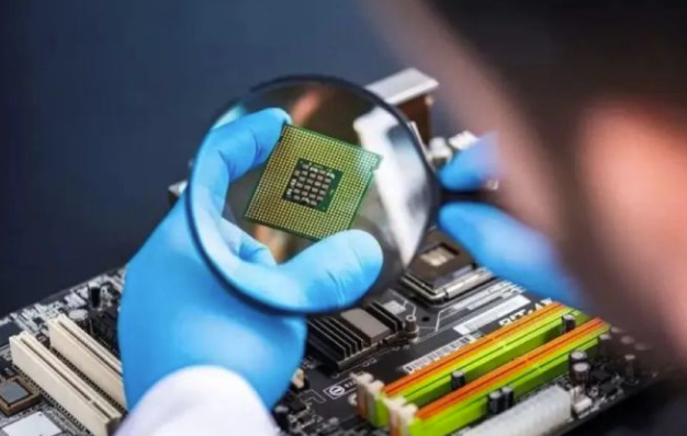
IC Testing PCB Manufacturing for Reliable Semiconductor Test Applications

As integrated circuits become more complex and performance-driven, IC testing PCB plays a critical role in ensuring functionality, reliability, and yield throughout the semiconductor lifecycle. From early-stage IC validation to high-volume production testing, IC testing PCBs provide the electrical interface between the device under test (DUT) and automated test equipment (ATE). A high-quality IC testing...