HomeTag

high density pcb - KKPCB

HDI PCB: High-Density Interconnect Technology for Advanced Electronics & Miniaturized Designs

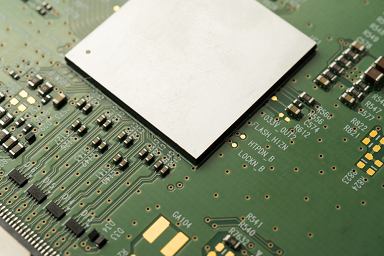
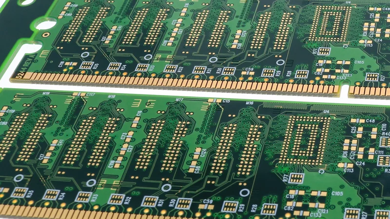
What is an HDI PCB? An HDI PCB (High-Density Interconnect PCB) is an advanced printed circuit board designed with higher wiring density per unit area, using technologies such as microvias, fine lines, and sequential lamination. Compared to conventional PCBs, an HDI PCB enables more compact layouts, improved electrical performance, and higher signal density, making it...

Microvia PCBs: Design, Reliability, and Engineering Trade-Offs Explained

Why Microvias Are Critical in Modern PCB Design As electronic devices continue to shrink while performance demands increase, traditional through-hole vias become a limiting factor. Microvias solve this by enabling high-density interconnects with shorter electrical paths. They are essential when: BGA pitch ≤ 0.8 mm (especially ≤ 0.5 mm) Routing congestion limits layout feasibility High-speed...

Buried Via PCBs: Strategic Layer Interconnects for High-Performance Designs

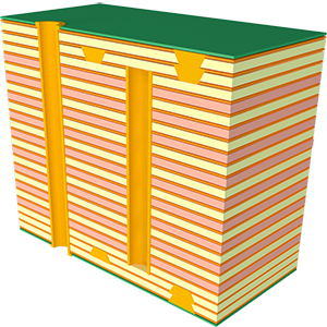
Why Buried Vias Matter As electronic systems become more compact and performance-driven, traditional via structures are no longer sufficient for complex routing requirements. A Buried Via PCB enables connections only between internal layers, eliminating unnecessary vertical paths through the entire board. This design approach is not just about saving space—it is about engineering control over...