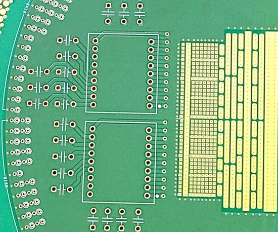
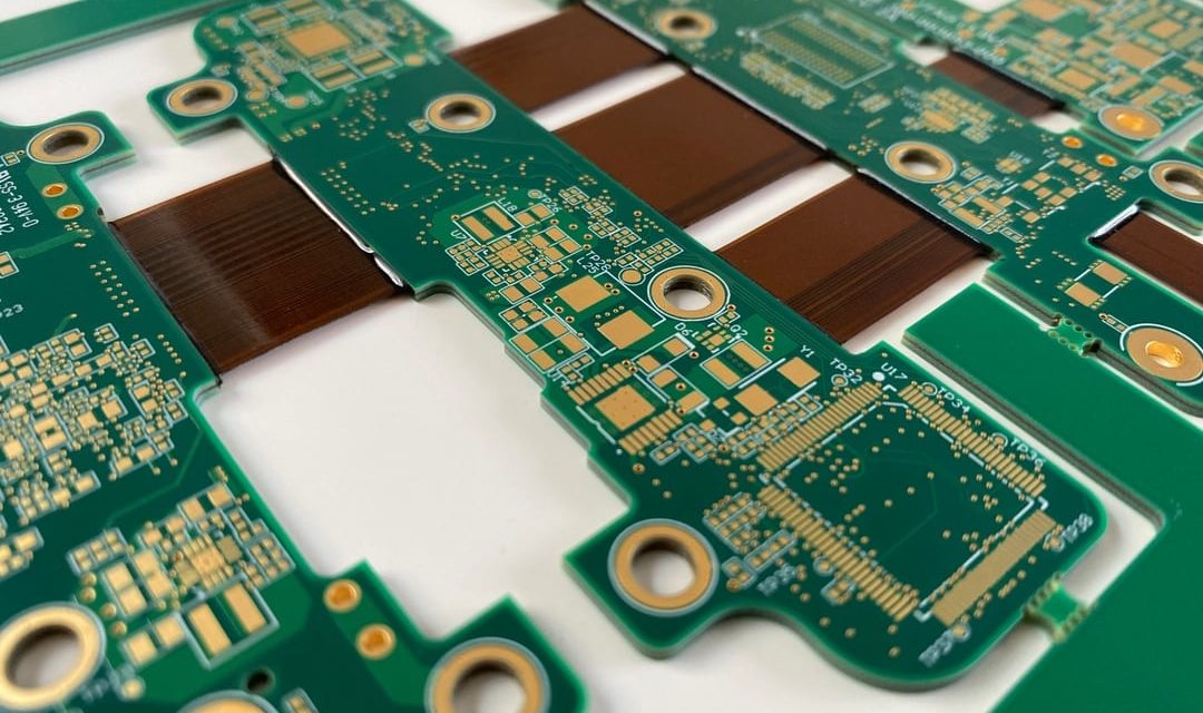
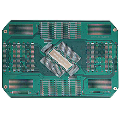
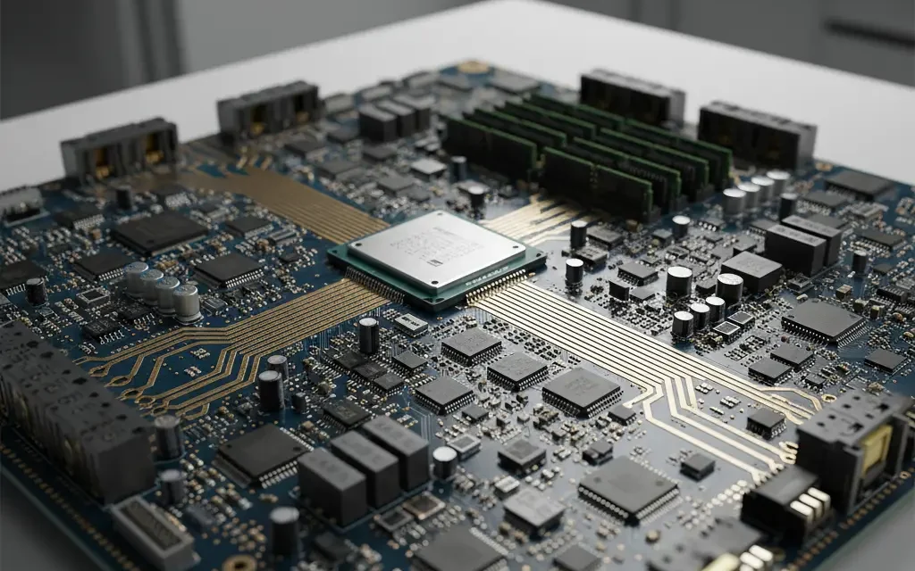
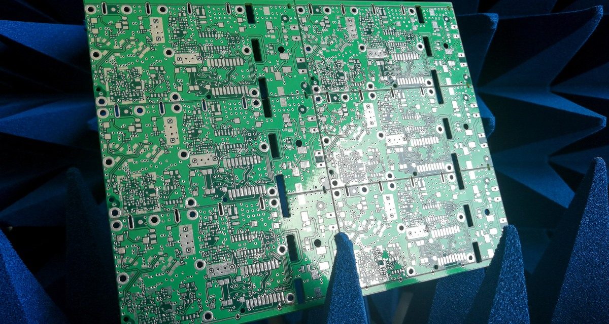
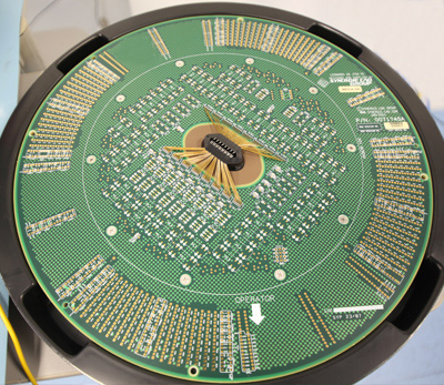
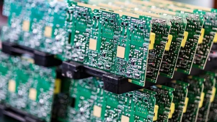
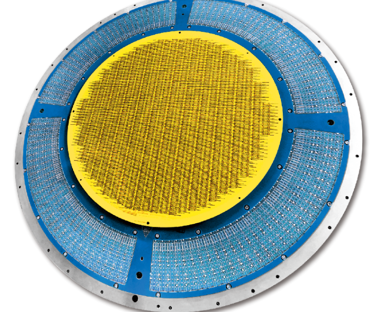
PCB Design Services | Professional PCB Layout & Design - KKPCB
 
HomeCategory

PCB Design Services | Professional PCB Layout & Design - KKPCB

Optimize Low-Loss Signal Chains and EMI Control Using RF Transceiver PCB Designs for High-Frequency Communication Systems

High-frequency communication systems—from 5G NR radios and phased-array front ends to satellite downlink modules and wideband radar—rely on precisely engineered RF Transceiver PCB architectures to maintain low-loss signal chains, stable phase performance, and strong EMI suppression. As operating frequencies rise into sub-6 GHz, C-band, Ku-band, Ka-band and even mmWave ranges, the electrical behavior of the...

High-Frequency Precision and Phase-Stable Performance Enabled by Advanced RF Transceiver PCB Architectures

Modern wireless systems—from satellite communication payloads to 5G/6G infrastructure and defense-grade radar—depend on the precision, stability, and reliability of RF Transceiver PCB architectures. As operating frequencies rise into the sub-6 GHz, Ku-, Ka-, and mmWave bands, the RF Transceiver PCB becomes the defining foundation for signal integrity, phase coherence, and power efficiency. High-frequency electronics demand...

High-Reliability Satellite PCB Engineering for Next-Generation RF, Digital and Power Payloads in LEO/MEO/GEO Space Systems

Satellite PCB: The Structural, Thermal, and RF Backbone of Modern Space Systems Modern satellites—whether operating in LEO constellations, MEO navigation networks, or GEO communication platforms—depend entirely on the reliability of their Satellite PCB. The Satellite PCB is not simply a circuit board; it is a mission-critical aerospace PCB platform engineered to manage high-frequency RF routing,...

Optimize Thermal Reliability Using High-Density Satellite PCB Stackups in Next-Generation LEO Constellation Terminals

LEO constellation terminals—whether phased-array user antennas, gateway stations, or compact mobile terminals—are being pushed toward wideband RF performance, higher transmit power, and increasingly integrated architectures.This raises a persistent engineering challenge: how to maintain thermal reliability inside a multilayer high-density PCB where RF, digital, and power systems coexist in tight proximity. At orbital altitudes, temperature swings...

Precision Impedance Control and Low-Loss High-Frequency Routing Using RO5880 PCB for Advanced Radar and 5G Modules

High-frequency radar and 5G modules demand precise impedance control, low insertion loss, and phase-stable signal propagation across dense multilayer architectures. Any deviation in Dk/Df, surface roughness, or stackup alignment can lead to signal distortion, beam misalignment, and reduced link margin. RO5880 PCB laminates (Dk = 2.2 ± 0.02, Df = 0.0009 @10 GHz) provide ultra-low...

Design Next-Gen Satellite Communication Systems with RO4835 PCB for Precise Impedance Control and Wideband Consistency

Satellite communication systems require ultra-stable RF performance across wide frequency bands, often spanning Ka- and Ku-bands. Maintaining precise impedance control, minimal insertion loss, and consistent phase response is critical for antenna feeds, transceivers, and payload modules. RO4835 PCB laminates (Dk = 3.48 ± 0.03, Df = 0.0037 @10 GHz) offer low-loss, thermally stable dielectric properties,...

Optimize Dielectric Stability and Low-Df Transmission with Duroid 5880 PCB Architectures for 10–67 GHz RF Subsystems

RF subsystems operating from 10 to 67 GHz—spanning 5G mmWave, satellite links, and aerospace communication modules—demand ultra-stable dielectric properties and minimal signal loss. Any Dk/Df variation or thermal-induced impedance drift directly degrades signal integrity, phase coherence, and overall RF system efficiency. Duroid 5880 PCB laminates (Dk = 2.2 ± 0.02, Df = 0.0009 @10 GHz)...

Accelerate PCB Quotation Requests with Complete Gerber, BOM, Stackup and Material Specifications

Fast and accurate PCB quotation is no longer a luxury—it is a critical enabler for modern hardware development. Whether the goal is prototype validation or high-volume mass production, incomplete design data often leads to delays, miscommunication, and multiple rounds of clarification. By providing complete engineering files such as the Gerber, BOM, stackup, and material specifications,...

Shorten R&D Cycles with Cost-Optimized, High-Reliability PCB Prototype Solutions for Rapid Electronics Development

Rapid electronics development has entered an era where design cycles are measured not in months but in weeks. From IoT edge devices to next-generation communication modules and automotive sensing platforms, engineers must iterate faster while maintaining electrical performance, manufacturability, and long-term reliability. PCB prototypes sit at the heart of this acceleration. When engineered correctly, they...

Enhance Phase Coherence and Thermal Stability in RF Transceiver PCB Stackups for Multi-Band Wireless Modules

Multi-band wireless modules are moving toward increasingly complex RF transceiver architectures, supporting simultaneous operation across sub-6 GHz, C-band, and mmWave channels. As bandwidth expands and carrier aggregation becomes standard, the performance of the RF transceiver PCB becomes a controlling factor in overall system efficiency. Maintaining phase coherence, thermal stability, and low-loss RF routing requires PCB...