KKPCB Blog – PCB & PCBA Insights, News, and Tips - KKPCB
 

Blog

Explore the KKPCB Blog for the latest PCB manufacturing and assembly news, industry insights, expert tips, and technology trends, helping you stay informed and optimize your electronics projects.
Optimize Beamforming Accuracy and Ultra-Low-Loss RF Propagation Using High-Frequency mmWave Module PCB Architectures for 28–60 GHz Wireless Platforms

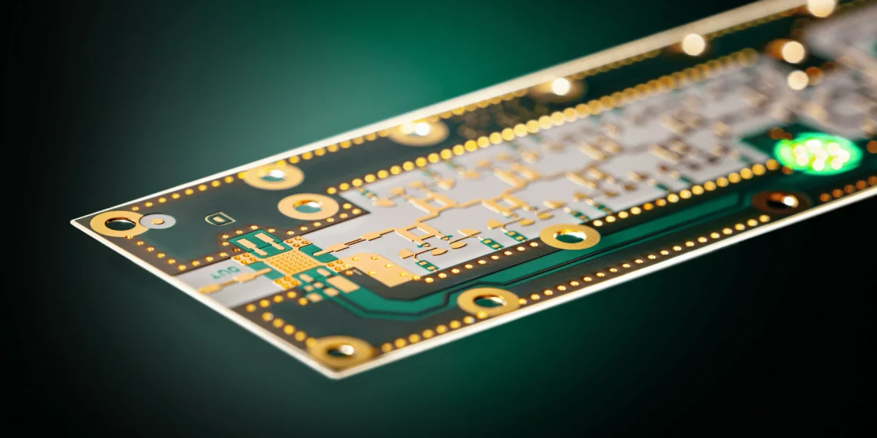
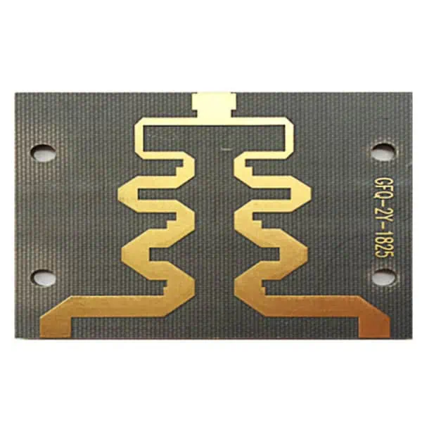
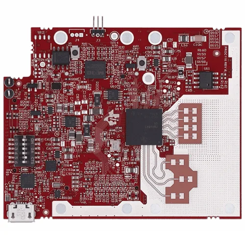
High-frequency mmWave module PCB architectures define the performance boundary of 28–60 GHz wireless platforms, where beamforming accuracy, ultra-low-loss routing, and tight impedance control determine every detail of system efficiency. In dense phased-array units, even microscopic changes in Dk/Df, copper roughness, dielectric uniformity, or via transition geometry produce measurable degradation in beam steering vectors, noise floors,...

Improve Multi-Gigabit Transmission and Low-Loss Routing Through Impedance Controlled PCB Engineering for Data Center Switches

Modern data center switches demand high-speed, multi-gigabit transmission across densely packed PCB layers. Maintaining low insertion loss, tight impedance control, and minimal crosstalk is critical to guarantee reliable signal integrity, reduce latency, and preserve network throughput. Impedance-controlled PCB architectures provide predictable high-frequency performance for differential pair routing and dense multilayer stackups. KKPCB leverages precision lamination,...

Minimize Crosstalk and Maintain Impedance Precision Using Advanced Blind Via PCB Layouts in 5G mmWave Systems

5G mmWave hardware doesn’t leave much room for layout mistakes. When operating above 24 GHz, a few microns of misalignment, a poorly shaped via stub, or an uncontrolled dielectric transition can collapse RF integrity. That is why advanced blind via PCB layouts have become a core enabling technology for minimizing crosstalk, stabilizing impedance, and preserving...

Optimize RF Signal Integrity and Lightweight HDI UAV PCB Architectures for Next-Gen Drone Navigation Modules

Next-generation UAV systems—whether used for industrial IoT sensing, long-range inspection, autonomous mapping, or precision agriculture—depend on PCB platforms capable of delivering high-frequency RF accuracy, ultra-stable GNSS/GPS reception, multi-band communication reliability, and lightweight HDI construction. As flight durations extend and sensor payloads grow more complex, the PCB becomes the backbone that determines navigation precision, RF sensitivity,...

Unlock Ultra-Stable RF Propagation and Low-Loss Routing with Next-Gen Multilayer HF PCB Platforms for Dense mmWave Arrays

Dense mmWave arrays, commonly used in 5G massive MIMO, radar, and satellite phased arrays, require ultra-stable RF propagation, minimal insertion loss, and precise impedance control across multilayer interconnects. Thermal stress, mechanical vibration, and high-frequency crosstalk can severely degrade signal fidelity, phase alignment, and overall array performance. Next-generation multilayer HF PCB platforms leverage advanced dielectric laminates...

Boost High-Q Resonance and Ultra-Stable Impedance Control with High-Frequency Sensor PCB Structures for Aerospace Navigation Sensors

Aerospace navigation sensors operate in a realm where the margin for error is essentially zero. Whether guiding autonomous aircraft, stabilizing flight control modules, or supporting satellite-assisted positioning, these sensors rely on high-frequency PCB platforms engineered for absolute electrical stability. Achieving high-Q resonance and ultra-consistent impedance is not just a design preference—it is the foundation of...

Reinforce Shock Reliability and High-Frequency Integrity Through Ruggedized mmWave Module PCB Designs for Harsh-Environment Communication Terminals

Harsh-environment communication terminals—used in battlefield radios, mining telemetry units, emergency response networks, and remote industrial gateways—depend on mmWave Module PCB architectures that can preserve signal integrity, impedance accuracy, and structural reliability under extreme stress. High-frequency circuits operating from 24 GHz to 71 GHz experience sensitivity far greater than conventional RF PCB designs, making material stability,...

Optimize Thermal Resilience and Multi-Layer Signal Fidelity with Megtron 7 PCB Stackups in High-Performance Computing Modules

High-performance computing modules in data centers, AI accelerators, and HPC servers operate with dense multi-layer interconnects and high-frequency signaling. Signal degradation, thermal hotspots, and impedance drift can severely impact throughput and reliability. Megtron 7 PCB laminates offer low-loss dielectric properties, tight Dk/Df tolerances, and high thermal conductivity, enabling reliable high-speed signal transmission in complex multi-layer...

Achieve Ultra-Stable Dk/Df and Low-Loss Performance with RO4835 PCB Architectures for High-Density 5G Massive-MIMO Radio Units

Next-generation 5G massive-MIMO radio units require high-density PCB designs that maintain ultra-consistent dielectric constant (Dk) and dissipation factor (Df) across all layers. Any variation in Dk/Df can lead to impedance mismatches, phase errors, and RF signal degradation, negatively affecting beamforming accuracy and spectral efficiency. RO4835 PCB laminates (Dk = 3.48 ± 0.03, Df = 0.0037...

Enhance Signal Accuracy and Low-Noise Stability with High Frequency Sensor PCB Platforms for Industrial IoT Detection Systems

Industrial IoT detection systems rely on a dense network of sensors for accurate monitoring of environmental parameters, machinery status, and process analytics. High frequency sensor PCBs must maintain low insertion loss, high signal-to-noise ratio, and phase-stable routing across multiple sensor channels to ensure reliable data acquisition. High frequency sensor PCB laminates (Dk = 3.2 ±...