KKPCB Blog – PCB & PCBA Insights, News, and Tips - KKPCB
 

Blog

Explore the KKPCB Blog for the latest PCB manufacturing and assembly news, industry insights, expert tips, and technology trends, helping you stay informed and optimize your electronics projects.
Boost Multi-Sensor Processing Efficiency Using High-Density UAV PCB Designs in Intelligent Aerial Surveillance Platforms

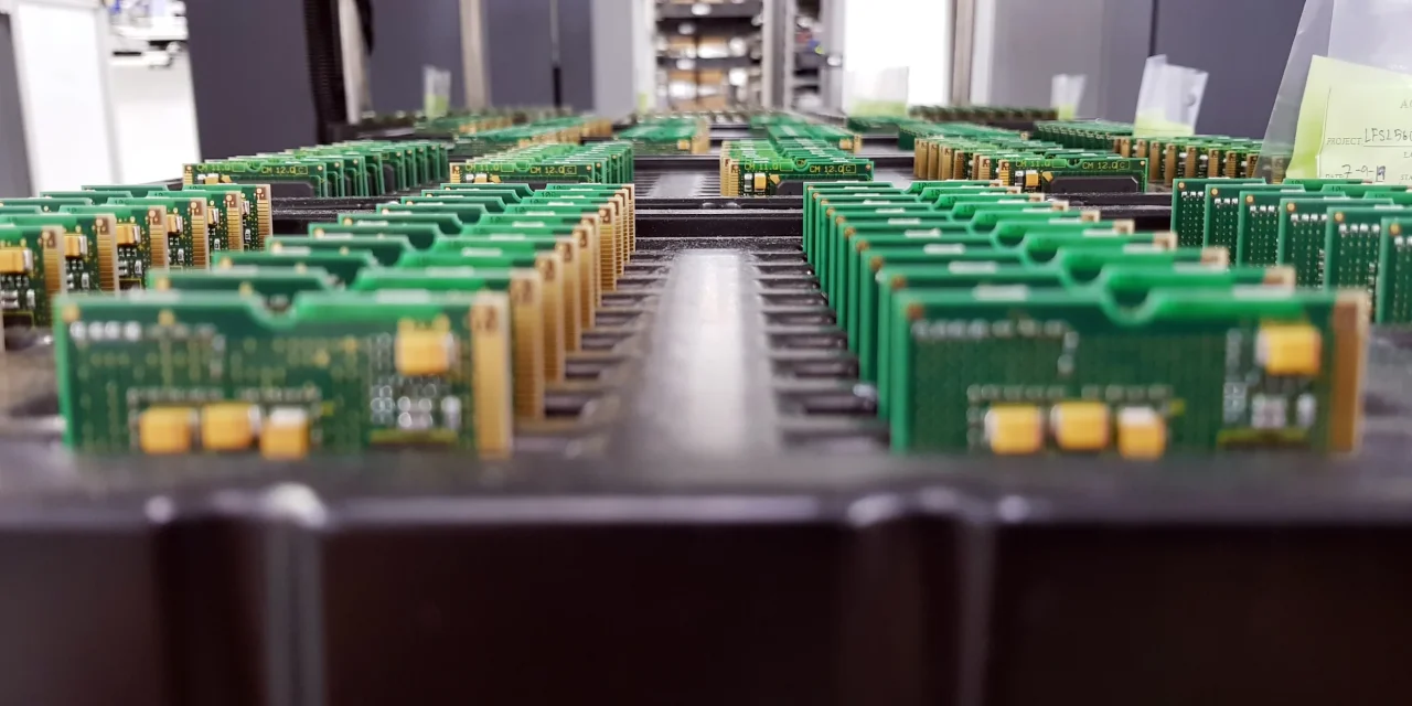
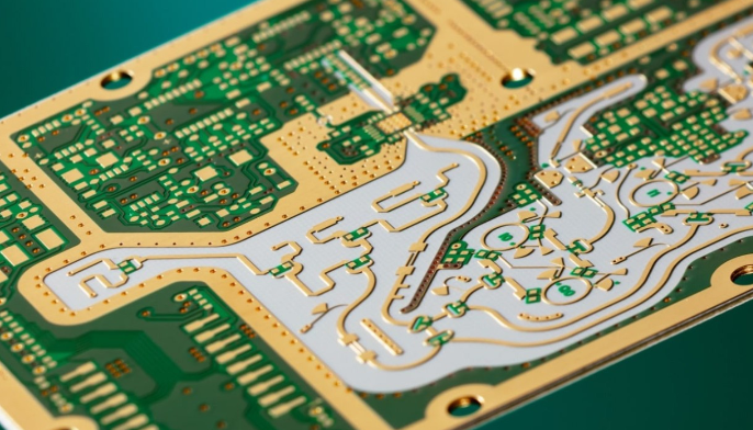
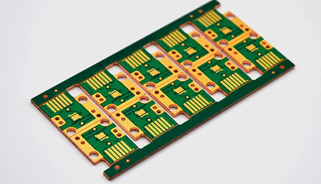
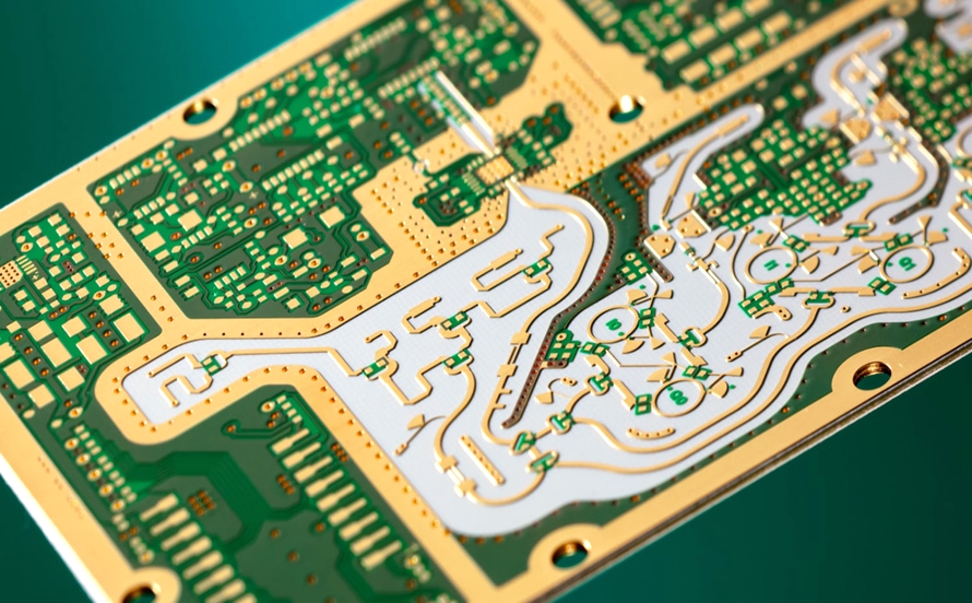
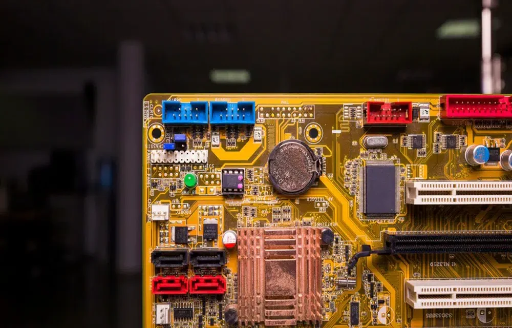
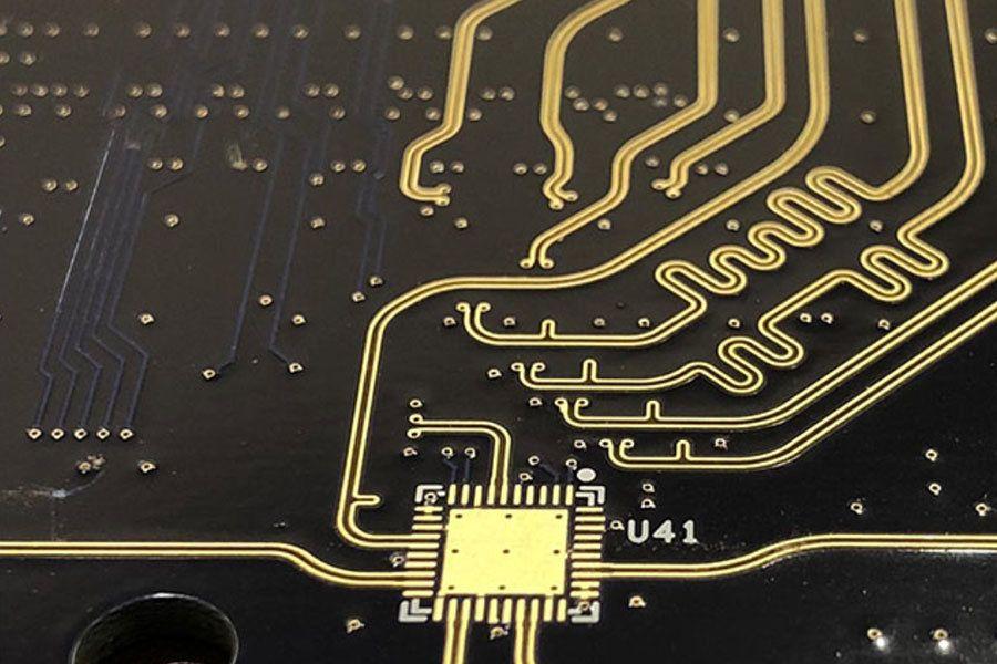
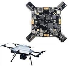
In next-generation intelligent aerial surveillance platforms, UAV manufacturers face increasing demands for real-time data fusion, long-range imaging, high-throughput RF links, and multi-sensor synchronization. These requirements place enormous pressure on the UAV PCB architecture, especially in compact airframes where thermal, mechanical, and electromagnetic constraints are all tightly coupled. This is why high-density PCB design (HDI PCB),...

Maximize RF Power Handling and Phase Stability Using RO4350B PCB Laminates in High-Frequency Antenna Modulegs

Modern wireless systems—from 5G radio units and phased-array antenna modules to automotive radar and satellite communication terminals—demand PCBs that deliver high RF power handling, exceptional phase stability, and ultra-low loss. As antenna modules continue to shrink while operating at higher frequencies, selecting the correct laminate becomes a mission-critical design decision. Among all mid-frequency RF substrates,...

Enhance Signal Integrity and Thermal Reliability in Multilayer Blind Via PCBs for High-Density RF Modules

High-density RF modules in 5G base stations, satellite payloads, and advanced IoT systems require compact multilayer PCBs with precise signal routing, minimal crosstalk, and high thermal resilience. Blind via technology allows for efficient vertical interconnects while reducing PCB stackup thickness, improving high-frequency performance, and maintaining signal integrity across densely packed layers. KKPCB integrates precision lamination,...

Boost RF Power Handling and Minimize Joule Heating Using Heavy Copper PCB Laminates in High-Power Telecom Amplifiers

High-power telecom amplifiers in 4G/5G base stations, satellite uplinks, and RF power transmitters operate under extreme currents and elevated temperatures. Maintaining low insertion loss, minimized Joule heating, and stable impedance is critical to achieve high RF efficiency, thermal reliability, and signal integrity. Heavy copper PCB laminates (copper thickness 3–6 oz, Dk ~4.0, low Df @10...

Reduce Insertion Loss and Enhance Power Efficiency Using Low Loss PCB Designs for Satellite Communication Payloads

Satellite communication payloads demand high-frequency RF stability, minimal insertion loss, and optimized power efficiency across densely packed multilayer PCBs. Signal integrity degradation, EMI coupling, or thermal hotspots can compromise link margin, telemetry accuracy, and antenna performance. Low loss PCB materials, such as ceramic-reinforced laminates or PTFE-based RF substrates, provide stable dielectric constant (Dk) and low...

Enhance Power Density and EMI Immunity Using Multilayer UAV PCB Stackups for Autonomous Flight Control Systems

Autonomous UAV flight control systems demand high power density PCB designs capable of handling dense interconnects, high-frequency control signals, and EMI-sensitive power circuits. Compact UAV architectures leave minimal space for routing, making multilayer PCB stackups essential for maintaining signal fidelity, phase stability, and electromagnetic compatibility. Multilayer UAV PCBs enable segregated power and control planes, optimized...

Optimize Phase-Stable High-Frequency Routing with Blind Via PCB Architectures in Compact Satellite Communication Payloads

Compact satellite communication payloads require precise, phase-stable RF routing to maintain signal fidelity and low insertion loss across high-frequency channels. The limited space and high-density requirements make blind via architectures essential for multilayer PCBs, enabling signal interconnects without penetrating all layers, reducing parasitic capacitance, and controlling crosstalk. Blind via PCBs allow compact routing of RF...

Accelerate Your PCB Quotation Request for Prototypes and Mass Production with Complete Design Files and Specs

A fast and accurate PCB quotation is critical for electronics designers, hardware engineers, and product managers who are planning prototypes or mass production runs. Providing complete design files and specifications, including Gerber files, Bill of Materials (BOM), PCB layer count, and manufacturing details, allows manufacturers to deliver precise, timely, and optimized PCB pricing. Without complete...

Optimize Beamforming Accuracy and Ultra-Low-Loss RF Propagation Using High-Frequency mmWave Module PCB Architectures for 28–60 GHz Wireless Platforms

High-frequency mmWave module PCB architectures define the performance boundary of 28–60 GHz wireless platforms, where beamforming accuracy, ultra-low-loss routing, and tight impedance control determine every detail of system efficiency. In dense phased-array units, even microscopic changes in Dk/Df, copper roughness, dielectric uniformity, or via transition geometry produce measurable degradation in beam steering vectors, noise floors,...

Improve Multi-Gigabit Transmission and Low-Loss Routing Through Impedance Controlled PCB Engineering for Data Center Switches

Modern data center switches demand high-speed, multi-gigabit transmission across densely packed PCB layers. Maintaining low insertion loss, tight impedance control, and minimal crosstalk is critical to guarantee reliable signal integrity, reduce latency, and preserve network throughput. Impedance-controlled PCB architectures provide predictable high-frequency performance for differential pair routing and dense multilayer stackups. KKPCB leverages precision lamination,...