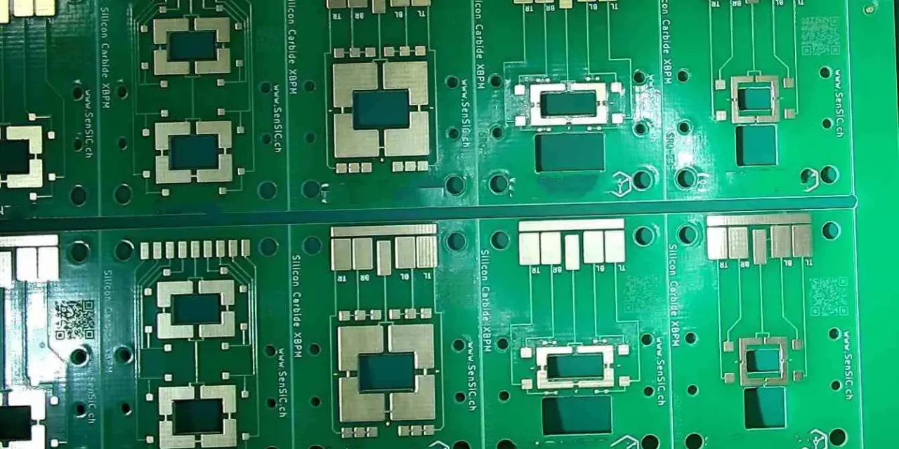
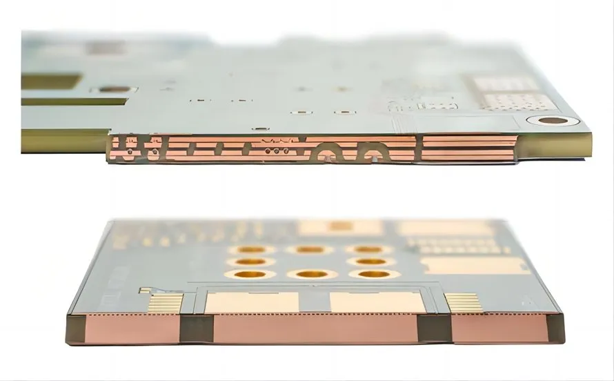
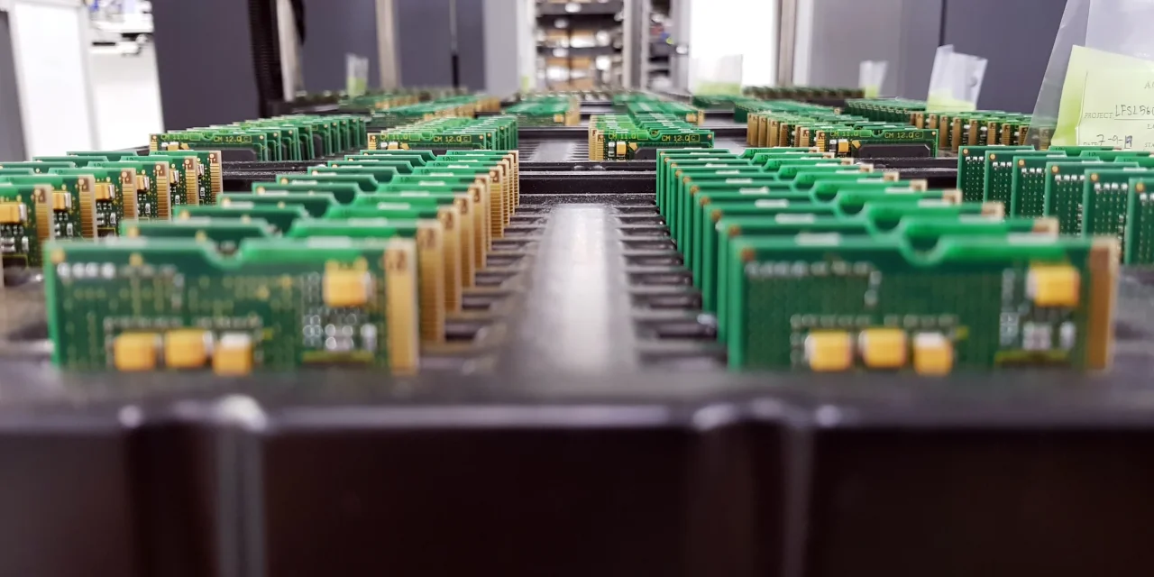
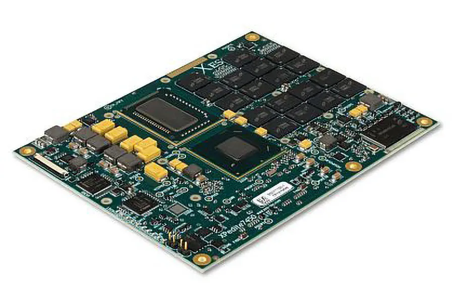
KKPCB Blog – PCB & PCBA Insights, News, and Tips - KKPCB
 

Blog

Explore the KKPCB Blog for the latest PCB manufacturing and assembly news, industry insights, expert tips, and technology trends, helping you stay informed and optimize your electronics projects.
PCB Design and Fabrication for Millimeter-Wave Circuits (Part 1)

Key Points of Millimeter-Wave Applications—Phase Accuracy Affected by Multiple Variables From anti-collision radar systems used in autonomous vehicles to the fifth-generation (5G) high data rate New Radio (NR) networks, the application of millimeter-wave (mmWave) circuits is growing rapidly. Many applications are pushing the operating frequency bands to higher frequencies (such as >24GHz). However, for circuits with shorter...

Microvia Reliability in High-Density Designs

As high-density interconnect (HDI) designs with larger layer counts become more prevalent, the use of microvias is increasing. In builds with 3+N+3 or larger configurations, sequential lamination now often relies on skipped vias, staggered microvias, and stacked microvias. However, one of the key challenges is that microvias are more susceptible to failure than plated through-holes. The small...

Copper Current Density in PCB Design

Copper current density refers to the amount of continuous current flowing through a copper trace on a PCB. According to Joule or Ohmic heating principles (represented as VI or I²R), any conductive material generates heat, leading to a gradual temperature rise in both the conductor and its surroundings. Managing copper current density is critical to...

PCB Layout Planning – Packages and Routing

PCB layout planning is a critical phase in the design process, enabling engineers to save time and ensure a structured approach to package management, component placement, and routing. Proper planning ensures that the design meets electrical, spacing, and physical requirements before moving to the actual layout stage. This article explores key aspects of PCB layout planning, focusing on footprint management, routing strategies,...

PCB Design For Military & Aerospace Applications

Military and aerospace PCBs must adhere to intensely high standards to ensure their safety and functionality in the extreme conditions they’re used in. For this reason, PCB design for military and aerospace applications requires incredibly stringent guidelines with built in redundancy, extra safety, and stringent tolerances, minimizing risk of failure. General PCB Design Tips for Military and Aerospace Applications...

RF Via Transitions in High-Speed Designs: Best Practices and Considerations

In high-speed and RF PCB designs, controlling trace impedance is critical, but the role of RF via transitions is often underestimated. Vias, which connect signals between layers, can introduce impedance mismatches, signal reflections, and losses, especially at high frequencies. Proper design and optimization of via transitions are essential to maintain signal integrity and ensure reliable performance in RF and...

How to Create a Variable Power Supply PCB Layout

A variable power supply allows the user to vary and adjust the desired output voltage and current. This type of power supply circuit includes an adjustable voltage regulator that can be set according to a specified input. An adjustable voltage regulator features both line regulation and load regulation. Unlike fixed power supplies that provide a...

Advanced PCB Footprint Generator: Key to Efficient PCB Design

Creating a robust component library is one of the most challenging yet critical aspects of PCB design. The quality of the library, which includes schematic symbols, PCB footprints, and 3D models, directly impacts the success of your board development. Among these, the PCB footprint plays a pivotal role in determining whether your board can be manufactured and...

Optimizing PCB Trace Thickness vs. Current Capacity

The relationship between PCB trace thickness and current capacity is a critical aspect of PCB design. Properly sizing traces ensures that they can handle the required current without overheating, which is essential for the reliability and functionality of the circuit. This article explores the key considerations for selecting trace thickness, the impact of copper weight, and...

PCB Routing: Best Practices for Ensuring Signal Integrity and Performance

Printed Circuit Board (PCB) routing is a critical aspect of electronic design, ensuring that electrical signals are transmitted efficiently and reliably between components. Proper routing minimizes interference, maintains signal integrity, and meets design requirements such as impedance control and thermal management. This article outlines the best practices for PCB routing, focusing on optimizing performance and ensuring signal integrity....